D6417760BP200ADV Renesas Electronics America, D6417760BP200ADV Datasheet - Page 82
D6417760BP200ADV
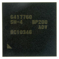
Manufacturer Part Number
D6417760BP200ADV
Description
IC SUPER H MPU ROMLESS 256BGA
Manufacturer
Renesas Electronics America
Series
SuperH® SH7750r
Datasheet
1.D6417760BP200ADV.pdf
(1418 pages)
Specifications of D6417760BP200ADV
Core Processor
SH-4
Core Size
32-Bit
Speed
200MHz
Connectivity
Audio Codec, CAN, EBI/EMI, FIFO, I²C, MFI, MMC, SCI, Serial Sound, SIM, SPI, USB
Peripherals
DMA, LCD, POR, WDT
Number Of I /o
69
Program Memory Type
ROMless
Ram Size
48K x 8
Voltage - Supply (vcc/vdd)
1.4 V ~ 1.6 V
Data Converters
A/D 4x10b
Oscillator Type
Internal
Operating Temperature
-40°C ~ 85°C
Package / Case
256-BGA
Lead Free Status / RoHS Status
Lead free / RoHS Compliant
Eeprom Size
-
Program Memory Size
-
Available stocks
Company
Part Number
Manufacturer
Quantity
Price
Company:

Part Number:
D6417760BP200ADV
Manufacturer:
Renesas Electronics America
Quantity:
10 000


Table 26.6
Table 26.7
Section 27 Multifunctional Interface (MFI)
Table 27.1
Table 27.2
Table 27.2
Table 27.3
Table 27.4
Table 27.5
Section 28 User Debug Interface (H-UDI)
Table 28.1
Table 28.2
Table 28.3
Table 28.4
Table 28.4
Table 28.4
Section 29 A/D Converter (ADC)
Table 29.1
Table 29.2
Table 29.2
Table 29.3
Table 29.4
Table 29.5
Table 29.6
Table 29.7
Table 29.8
Section 30 LCD Controller (LCDC)
Table 30.1
Table 30.2
Table 30.2
Table 30.3
Table 30.4
Table 30.5
Table 30.6
Table 30.7
Rev. 2.00 Feb. 12, 2010 Page lxxx of lxxxii
REJ09B0554-0200
Card States in which Command Sequence Is Halted ............................................. 951
MMCIF Interrupt Sources...................................................................................... 990
Pin Configuration ................................................................................................... 999
Register Configuration (1).................................................................................... 1000
Register Configuration (2).................................................................................... 1001
MFI Operations .................................................................................................... 1012
Access to MFIIDX and MFIGSR......................................................................... 1012
Memory Map........................................................................................................ 1013
Pin Configuration ................................................................................................. 1021
Commands Supported by Boundary-Scan TAP Controller.................................. 1024
SDBSR Configuration.......................................................................................... 1024
Register Configuration (1).................................................................................... 1032
Register Configuration (2).................................................................................... 1032
Register Configuration (3).................................................................................... 1033
Pin Configuration ................................................................................................. 1041
Register Configuration (1).................................................................................... 1042
Register Configuration (2).................................................................................... 1042
Analog Input Channels and Corresponding A/D Conversion Data Registers ...... 1043
A/D Conversion Time .......................................................................................... 1054
Relationship between Clock Division Ratio and Usable Input Clock
Frequency............................................................................................................. 1059
AD Conversion Time ........................................................................................... 1060
ADST Transition Period....................................................................................... 1060
Setting between Pck and Clock Division Ratio.................................................... 1061
Pin Configuration ................................................................................................. 1064
Register Configuration (1).................................................................................... 1065
Register Configuration (2).................................................................................... 1066
I/O Clock Frequency and Clock Division Ratio................................................... 1069
Display Resolutions when Using Display Rotation ............................................. 1093
Available Power-Supply Control-Sequence Periods at Typical Frame Rates ...... 1101
LCDC Operating Modes ...................................................................................... 1102
LCD Module Power-Supply States ...................................................................... 1102
Related parts for D6417760BP200ADV
Image
Part Number
Description
Manufacturer
Datasheet
Request
R

Part Number:
Description:
KIT STARTER FOR M16C/29
Manufacturer:
Renesas Electronics America
Datasheet:

Part Number:
Description:
KIT STARTER FOR R8C/2D
Manufacturer:
Renesas Electronics America
Datasheet:

Part Number:
Description:
R0K33062P STARTER KIT
Manufacturer:
Renesas Electronics America
Datasheet:

Part Number:
Description:
KIT STARTER FOR R8C/23 E8A
Manufacturer:
Renesas Electronics America
Datasheet:

Part Number:
Description:
KIT STARTER FOR R8C/25
Manufacturer:
Renesas Electronics America
Datasheet:

Part Number:
Description:
KIT STARTER H8S2456 SHARPE DSPLY
Manufacturer:
Renesas Electronics America
Datasheet:

Part Number:
Description:
KIT STARTER FOR R8C38C
Manufacturer:
Renesas Electronics America
Datasheet:

Part Number:
Description:
KIT STARTER FOR R8C35C
Manufacturer:
Renesas Electronics America
Datasheet:

Part Number:
Description:
KIT STARTER FOR R8CL3AC+LCD APPS
Manufacturer:
Renesas Electronics America
Datasheet:
Part Number:
Description:
KIT STARTER FOR RX610
Manufacturer:
Renesas Electronics America
Datasheet:

Part Number:
Description:
KIT STARTER FOR R32C/118
Manufacturer:
Renesas Electronics America
Datasheet:

Part Number:
Description:
KIT DEV RSK-R8C/26-29
Manufacturer:
Renesas Electronics America
Datasheet:

Part Number:
Description:
KIT STARTER FOR SH7124
Manufacturer:
Renesas Electronics America
Datasheet:

Part Number:
Description:
KIT STARTER FOR H8SX/1622
Manufacturer:
Renesas Electronics America
Datasheet:

Part Number:
Description:
KIT DEV FOR SH7203
Manufacturer:
Renesas Electronics America
Datasheet: