D6417760BP200ADV Renesas Electronics America, D6417760BP200ADV Datasheet - Page 657
D6417760BP200ADV
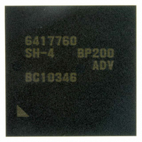
Manufacturer Part Number
D6417760BP200ADV
Description
IC SUPER H MPU ROMLESS 256BGA
Manufacturer
Renesas Electronics America
Series
SuperH® SH7750r
Datasheet
1.D6417760BP200ADV.pdf
(1418 pages)
Specifications of D6417760BP200ADV
Core Processor
SH-4
Core Size
32-Bit
Speed
200MHz
Connectivity
Audio Codec, CAN, EBI/EMI, FIFO, I²C, MFI, MMC, SCI, Serial Sound, SIM, SPI, USB
Peripherals
DMA, LCD, POR, WDT
Number Of I /o
69
Program Memory Type
ROMless
Ram Size
48K x 8
Voltage - Supply (vcc/vdd)
1.4 V ~ 1.6 V
Data Converters
A/D 4x10b
Oscillator Type
Internal
Operating Temperature
-40°C ~ 85°C
Package / Case
256-BGA
Lead Free Status / RoHS Status
Lead free / RoHS Compliant
Eeprom Size
-
Program Memory Size
-
Available stocks
Company
Part Number
Manufacturer
Quantity
Price
Company:

Part Number:
D6417760BP200ADV
Manufacturer:
Renesas Electronics America
Quantity:
10 000


17.2
Table 17.1 shows the SCIF pin configuration. Since the pin functions are the same in each
channel, the channel number is omitted in the description below. The modem control pins are
available only in channels 1 and 2, and not in channel 0.
Table 17.1 Pin Configuration
Pin Name
Serial clock pin
Receive data pin
Transmit data pin
Modem control pin
Modem control pin
Note: These pins are made to function as serial pins by performing SCIF operation settings with
the C/A bit in SCSMR, the TE, RE, CKE1, and CKE0 bits in SCSCR, and the MCE bit in
SCFCR. Break state transmission and detection can be set in SCSPTR of the SCIF.
Input/Output Pins
Abbreviation
SCIF0_CLK to SCIF2_CLK
SCIF0_RXD to SCIF2_RXD
SCIF0_TXD to SCIF2_TXD
SCIF1_CTS, SCIF2_CTS
SCIF1_RTS, SCIF2_RTS
I/O
Input/Output
Input/Output
Input/Output
Input/Output
Input/Output
Rev. 2.00 Feb. 12, 2010 Page 573 of 1330
Function
Clock input/output
Receive data input
Transmit data output
Transmission enabled
Transmission request
REJ09B0554-0200
Related parts for D6417760BP200ADV
Image
Part Number
Description
Manufacturer
Datasheet
Request
R

Part Number:
Description:
KIT STARTER FOR M16C/29
Manufacturer:
Renesas Electronics America
Datasheet:

Part Number:
Description:
KIT STARTER FOR R8C/2D
Manufacturer:
Renesas Electronics America
Datasheet:

Part Number:
Description:
R0K33062P STARTER KIT
Manufacturer:
Renesas Electronics America
Datasheet:

Part Number:
Description:
KIT STARTER FOR R8C/23 E8A
Manufacturer:
Renesas Electronics America
Datasheet:

Part Number:
Description:
KIT STARTER FOR R8C/25
Manufacturer:
Renesas Electronics America
Datasheet:

Part Number:
Description:
KIT STARTER H8S2456 SHARPE DSPLY
Manufacturer:
Renesas Electronics America
Datasheet:

Part Number:
Description:
KIT STARTER FOR R8C38C
Manufacturer:
Renesas Electronics America
Datasheet:

Part Number:
Description:
KIT STARTER FOR R8C35C
Manufacturer:
Renesas Electronics America
Datasheet:

Part Number:
Description:
KIT STARTER FOR R8CL3AC+LCD APPS
Manufacturer:
Renesas Electronics America
Datasheet:
Part Number:
Description:
KIT STARTER FOR RX610
Manufacturer:
Renesas Electronics America
Datasheet:

Part Number:
Description:
KIT STARTER FOR R32C/118
Manufacturer:
Renesas Electronics America
Datasheet:

Part Number:
Description:
KIT DEV RSK-R8C/26-29
Manufacturer:
Renesas Electronics America
Datasheet:

Part Number:
Description:
KIT STARTER FOR SH7124
Manufacturer:
Renesas Electronics America
Datasheet:

Part Number:
Description:
KIT STARTER FOR H8SX/1622
Manufacturer:
Renesas Electronics America
Datasheet:

Part Number:
Description:
KIT DEV FOR SH7203
Manufacturer:
Renesas Electronics America
Datasheet: