D6417760BP200ADV Renesas Electronics America, D6417760BP200ADV Datasheet - Page 786
D6417760BP200ADV
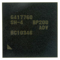
Manufacturer Part Number
D6417760BP200ADV
Description
IC SUPER H MPU ROMLESS 256BGA
Manufacturer
Renesas Electronics America
Series
SuperH® SH7750r
Datasheet
1.D6417760BP200ADV.pdf
(1418 pages)
Specifications of D6417760BP200ADV
Core Processor
SH-4
Core Size
32-Bit
Speed
200MHz
Connectivity
Audio Codec, CAN, EBI/EMI, FIFO, I²C, MFI, MMC, SCI, Serial Sound, SIM, SPI, USB
Peripherals
DMA, LCD, POR, WDT
Number Of I /o
69
Program Memory Type
ROMless
Ram Size
48K x 8
Voltage - Supply (vcc/vdd)
1.4 V ~ 1.6 V
Data Converters
A/D 4x10b
Oscillator Type
Internal
Operating Temperature
-40°C ~ 85°C
Package / Case
256-BGA
Lead Free Status / RoHS Status
Lead free / RoHS Compliant
Eeprom Size
-
Program Memory Size
-
Available stocks
Company
Part Number
Manufacturer
Quantity
Price
Company:

Part Number:
D6417760BP200ADV
Manufacturer:
Renesas Electronics America
Quantity:
10 000


Section 19 I
(5) Monitor the progress of data byte reception:
(a) Wait for a master event (the MDR bit in the master status register).
(b) Set the master control register 8Ah.
(c) Reset the MDR bit to 0.
(6) Wait for the end of transmission:
(a) Execute processing of the last byte receive interrupt (MDR), i.e., extract the data and clear
(b) Wait for the master device’s event (the MST bit in the master status register).
(c) Reset the MST bit to 0.
19.6.4
Operation example:
1. Set the clock rate to ICCCR.
2. Set the slave address, etc. to ICMAR.
3. Write transmission data to ICTXD (up to 16 bytes can be written).
4. Clear the TDFE flag.
5. ICMCR=H'0000 0009 (set ESG) //ESG=1, MIE=1, MDBS=0. (At this point, the slave address
6. Wait for MAT to be set to 1, and clear ESG, MAT, and MDE to 0. (Transmission data has
7. Wait for TDFE to be set to 1, and write subsequent transmit data to ICTXD.
8. Set FSB to 1 after 1 SCL clock period has completed and before 9 SCL clock periods have
9. Clear the TEND flag to 0.
Rev. 2.00 Feb. 12, 2010 Page 702 of 1330
REJ09B0554-0200
(Repeat)
Read data from the receive data register.
If next byte is to be the data immediately preceding the last byte transmitted by the slave
device, for the receive interrupt for the byte immediately preceding the last one-byte, i.e.,
MDR interrupt,
(Set the force stop control bit.)
MDR.
is output onto I
been output until FIFO becomes empty.)
ICFSR=H'0000 0000 (Clear the flag.)
completed after TDFE was set to 1.
(See figure 19.15)
Master Transmitter (FIFO Buffer Mode)
2
C Bus Interface
2
C bus.)
Related parts for D6417760BP200ADV
Image
Part Number
Description
Manufacturer
Datasheet
Request
R

Part Number:
Description:
KIT STARTER FOR M16C/29
Manufacturer:
Renesas Electronics America
Datasheet:

Part Number:
Description:
KIT STARTER FOR R8C/2D
Manufacturer:
Renesas Electronics America
Datasheet:

Part Number:
Description:
R0K33062P STARTER KIT
Manufacturer:
Renesas Electronics America
Datasheet:

Part Number:
Description:
KIT STARTER FOR R8C/23 E8A
Manufacturer:
Renesas Electronics America
Datasheet:

Part Number:
Description:
KIT STARTER FOR R8C/25
Manufacturer:
Renesas Electronics America
Datasheet:

Part Number:
Description:
KIT STARTER H8S2456 SHARPE DSPLY
Manufacturer:
Renesas Electronics America
Datasheet:

Part Number:
Description:
KIT STARTER FOR R8C38C
Manufacturer:
Renesas Electronics America
Datasheet:

Part Number:
Description:
KIT STARTER FOR R8C35C
Manufacturer:
Renesas Electronics America
Datasheet:

Part Number:
Description:
KIT STARTER FOR R8CL3AC+LCD APPS
Manufacturer:
Renesas Electronics America
Datasheet:
Part Number:
Description:
KIT STARTER FOR RX610
Manufacturer:
Renesas Electronics America
Datasheet:

Part Number:
Description:
KIT STARTER FOR R32C/118
Manufacturer:
Renesas Electronics America
Datasheet:

Part Number:
Description:
KIT DEV RSK-R8C/26-29
Manufacturer:
Renesas Electronics America
Datasheet:

Part Number:
Description:
KIT STARTER FOR SH7124
Manufacturer:
Renesas Electronics America
Datasheet:

Part Number:
Description:
KIT STARTER FOR H8SX/1622
Manufacturer:
Renesas Electronics America
Datasheet:

Part Number:
Description:
KIT DEV FOR SH7203
Manufacturer:
Renesas Electronics America
Datasheet: