HD6413003TF16V Renesas Electronics America, HD6413003TF16V Datasheet - Page 123
HD6413003TF16V
Manufacturer Part Number
HD6413003TF16V
Description
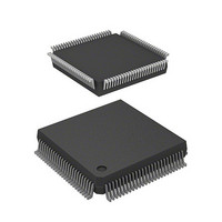
MCU 5V 0K PB-FREE 112-QFP
Manufacturer
Renesas Electronics America
Series
H8® H8/300Hr
Datasheet
1.D13003TF16V.pdf
(717 pages)
Specifications of HD6413003TF16V
Core Size
16-Bit
Oscillator Type
Internal
Core Processor
H8/300H
Speed
16MHz
Connectivity
SCI
Peripherals
DMA, PWM, WDT
Number Of I /o
50
Program Memory Type
ROMless
Ram Size
512 x 8
Voltage - Supply (vcc/vdd)
2.7 V ~ 5.5 V
Data Converters
A/D 8x10b
Operating Temperature
-20°C ~ 75°C
Package / Case
112-QFP
No. Of I/o's
58
Ram Memory Size
512Byte
Cpu Speed
16MHz
No. Of Timers
11
No. Of Pwm Channels
4
Digital Ic Case Style
QFP
Supply Voltage
RoHS Compliant
Controller Family/series
H8/300H
Rohs Compliant
Yes
Lead Free Status / RoHS Status
Lead free / RoHS Compliant
Eeprom Size
-
Program Memory Size
-
Lead Free Status / RoHS Status
Lead free / RoHS Compliant
Available stocks
Company
Part Number
Manufacturer
Quantity
Price
Company:

Part Number:
HD6413003TF16V
Manufacturer:
ITT
Quantity:
12 000
Company:
Part Number:
HD6413003TF16V
Manufacturer:
RENESAS
Quantity:
36
Part Number:
HD6413003TF16V
Manufacturer:
RENESAS/瑞萨
Quantity:
20 000


6.1.3 Input/Output Pins
Table 6-1 summarizes the bus controller’s input/output pins.
Table 6-1 Bus Controller Pins
Name
Chip select 0 to 7
Address strobe
Read
High write
Low write
Wait
Bus request
Bus acknowledge
6.1.4 Register Configuration
Table 6-2 summarizes the bus controller’s registers.
Table 6-2 Bus Controller Registers
Address*
H'FFEC
H'FFED
H'FFEE
H'FFEF
H'FFF3
Note: * Lower 16 bits of the address.
Name
Bus width control register
Access state control register
Wait control register
Wait state controller enable register
Bus release control register
Abbreviation
CS
AS
RD
HWR
LWR
WAIT
BREQ
BACK
0
to CS
7
I/O
Output
Output
Output
Output
Output
Input
Input
Output
Function
Strobe signals selecting areas 0 to 7
Strobe signal indicating valid address output on the
address bus
Strobe signal indicating reading from the external
address space
Strobe signal indicating writing to the external
address space, with valid data on the upper data
bus (D
Strobe signal indicating writing to the external
address space, with valid data on the lower data
bus (D
Wait request signal for access to external three-
state-access areas
Request signal for releasing the bus to an external
device
Acknowledge signal indicating the bus is released
to an external device
103
Abbrevi-
ation
ABWCR
ASTCR
WCR
WCER
BRCR
15
7
to D
to D
0
8
)
)
R/W
R/W
R/W
R/W
R/W
R/W
Modes 1 & 3 Modes 2 & 4
H'F3
H'FF
H'FF
H'FF
H'FE
Initial Value
H'00
H'FF
H'F3
H'FF
H'FE
Related parts for HD6413003TF16V
Image
Part Number
Description
Manufacturer
Datasheet
Request
R

Part Number:
Description:
KIT STARTER FOR M16C/29
Manufacturer:
Renesas Electronics America
Datasheet:

Part Number:
Description:
KIT STARTER FOR R8C/2D
Manufacturer:
Renesas Electronics America
Datasheet:

Part Number:
Description:
R0K33062P STARTER KIT
Manufacturer:
Renesas Electronics America
Datasheet:

Part Number:
Description:
KIT STARTER FOR R8C/23 E8A
Manufacturer:
Renesas Electronics America
Datasheet:

Part Number:
Description:
KIT STARTER FOR R8C/25
Manufacturer:
Renesas Electronics America
Datasheet:

Part Number:
Description:
KIT STARTER H8S2456 SHARPE DSPLY
Manufacturer:
Renesas Electronics America
Datasheet:

Part Number:
Description:
KIT STARTER FOR R8C38C
Manufacturer:
Renesas Electronics America
Datasheet:

Part Number:
Description:
KIT STARTER FOR R8C35C
Manufacturer:
Renesas Electronics America
Datasheet:

Part Number:
Description:
KIT STARTER FOR R8CL3AC+LCD APPS
Manufacturer:
Renesas Electronics America
Datasheet:
Part Number:
Description:
KIT STARTER FOR RX610
Manufacturer:
Renesas Electronics America
Datasheet:

Part Number:
Description:
KIT STARTER FOR R32C/118
Manufacturer:
Renesas Electronics America
Datasheet:

Part Number:
Description:
KIT DEV RSK-R8C/26-29
Manufacturer:
Renesas Electronics America
Datasheet:

Part Number:
Description:
KIT STARTER FOR SH7124
Manufacturer:
Renesas Electronics America
Datasheet:

Part Number:
Description:
KIT STARTER FOR H8SX/1622
Manufacturer:
Renesas Electronics America
Datasheet:

Part Number:
Description:
KIT DEV FOR SH7203
Manufacturer:
Renesas Electronics America
Datasheet: