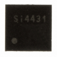
SI4431-A0-FM Silicon Laboratories Inc, SI4431-A0-FM Datasheet - Page 16

SI4431-A0-FM
Manufacturer Part Number
SI4431-A0-FM
Description
IC TXRX ISM 930MHZ 3.6V 20-QFN
Manufacturer
Silicon Laboratories Inc
Specifications of SI4431-A0-FM
Package / Case
20-QFN
Mfg Application Notes
Transitioning SI4430/31 to Rev B
Frequency
240MHz ~ 930MHz
Data Rate - Maximum
128kbps
Modulation Or Protocol
FSK, GFSK, OOK
Power - Output
13dBm
Sensitivity
-118dBm
Voltage - Supply
1.8 V ~ 3.6 V
Current - Receiving
18.5mA
Current - Transmitting
28mA
Data Interface
PCB, Surface Mount
Antenna Connector
PCB, Surface Mount
Operating Temperature
-40°C ~ 85°C
Number Of Receivers
2
Number Of Transmitters
1
Wireless Frequency
240 MHz to 930 MHz
Output Power
13 dBm
Operating Supply Voltage
1.8 V to 3.6 V
Maximum Operating Temperature
+ 85 C
Mounting Style
SMD/SMT
Maximum Supply Current
28 mA
Minimum Operating Temperature
- 40 C
Modulation
FSK, GFSK, OOK
Lead Free Status / RoHS Status
Lead free / RoHS Compliant
Applications
-
Memory Size
-
Lead Free Status / RoHS Status
Lead free / RoHS Compliant, Lead free / RoHS Compliant
Other names
336-1633-5
Available stocks
Company
Part Number
Manufacturer
Quantity
Price
Company:
Part Number:
SI4431-A0-FMR
Manufacturer:
SILICON
Quantity:
3 500
Part Number:
SI4431-A0-FMR
Manufacturer:
SILICONLABS/èٹ¯ç§‘
Quantity:
20 000
Si4431
2. Functional Description
The Si4431 is a 100% CMOS ISM wireless transceiver with continuous frequency tuning over the complete
240–930 MHz band. The wide operating voltage range of 1.8–3.6 V and low current consumption makes the
Si4431 and ideal solution for battery powered applications.
The Si4431 operates as a time division duplexing (TDD) transceiver where the device alternately transmits and
receives data packets. The device uses a single-conversion, image-reject mixer to downconvert the 2-level
FSK/GFSK/OOK modulated receive signal to a low IF frequency. Following a programmable gain amplifier (PGA)
the signal is converted to the digital domain by a high performance ADC allowing filtering, demodulation, slicing,
error correction, and packet handling to be performed in the built-in DSP increasing the receiver’s performance and
flexibility versus analog based architectures. The demodulated signal is then output to the system MCU through a
programmable GPIO or via the standard SPI bus by reading the 64-byte RX FIFO.
A single high precision local oscillator (LO) is used for both transmit and receive modes since the transmitter and
receiver do not operate at the same time. The LO is generated by an integrated VCO and Fractional-N PLL
synthesizer. The synthesizer is designed to support configurable data rates, output frequency, frequency deviation,
and Gaussian filtering at any frequency between 240–930 MHz. The transmit FSK data is modulated directly into
the data stream and can be shaped by a Gaussian low-pass filter to reduce unwanted spectral content.
The PA output power can be configured between –8 and +13 dBm in 3 dB steps. The PA is single-ended to allow
for easy antenna matching and low BOM cost. The PA incorporates automatic ramp-up and ramp-down control to
reduce unwanted spectral spreading. The Si4431 supports frequency hopping, TX/RX switch control, and antenna
diversity switch control to extend the link range and improve performance. Antenna diversity is completely
integrated into the Si4431 and can improve the system link budget by 8–10 dB, resulting in substantial range
increases depending on the environmental conditions.
The Si4431 is designed to work with a microcontroller, crystal, and a few passives to create a very low cost system
as shown Figure 1. Voltage regulators are integrated on-chip which allow for a wide range of operating supply
voltage conditions from +1.8 to +3.6 V. A standard 4-pin SPI bus is used to communicate with the microcontroller.
Three configurable general purpose I/Os are available for use to tailor towards the needs of the system. A more
complete list of the available GPIO functions is shown in "8. Auxiliary Functions" on page 55 but just to name a few,
microcontroller clock output, Antenna Diversity, POR, and specific interrupts. A limited number of passive
components are needed to match the LNA and PA.
The application shown in Figure 1 is designed for a system with an TX/RX direct-tie configuration without the use of
a TX/RX switch. Most lower power applications will use this configuration. A direct-tie reference design is available
from Silicon Laboratories applications support.
For applications seeking improved performance in the presence of multipath fading antenna diversity can be used.
Antenna diversity includes a switch to select the optimal antenna between a pair of antennas for improved
performance. The Antenna Diversity Control Algorithm is completely integrated into the chip. A complete Antenna
Diversity reference design is available from Silicon Laboratories applications support.
An application example with a separate RX and TX antenna is shown in Figure 31, “Split RF I/Os with Separated
TX and RX Connectors—Schematic,” on page 69. This example is used for testing of the TX and RX paths in a lab
environment and shows, conceptually, the matching of the TX and RX antennas.
16
Preliminary Rev. 0.4


