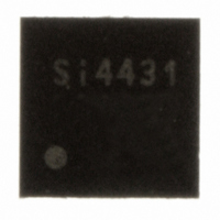
SI4431-A0-FM Silicon Laboratories Inc, SI4431-A0-FM Datasheet - Page 35

SI4431-A0-FM
Manufacturer Part Number
SI4431-A0-FM
Description
IC TXRX ISM 930MHZ 3.6V 20-QFN
Manufacturer
Silicon Laboratories Inc
Specifications of SI4431-A0-FM
Package / Case
20-QFN
Mfg Application Notes
Transitioning SI4430/31 to Rev B
Frequency
240MHz ~ 930MHz
Data Rate - Maximum
128kbps
Modulation Or Protocol
FSK, GFSK, OOK
Power - Output
13dBm
Sensitivity
-118dBm
Voltage - Supply
1.8 V ~ 3.6 V
Current - Receiving
18.5mA
Current - Transmitting
28mA
Data Interface
PCB, Surface Mount
Antenna Connector
PCB, Surface Mount
Operating Temperature
-40°C ~ 85°C
Number Of Receivers
2
Number Of Transmitters
1
Wireless Frequency
240 MHz to 930 MHz
Output Power
13 dBm
Operating Supply Voltage
1.8 V to 3.6 V
Maximum Operating Temperature
+ 85 C
Mounting Style
SMD/SMT
Maximum Supply Current
28 mA
Minimum Operating Temperature
- 40 C
Modulation
FSK, GFSK, OOK
Lead Free Status / RoHS Status
Lead free / RoHS Compliant
Applications
-
Memory Size
-
Lead Free Status / RoHS Status
Lead free / RoHS Compliant, Lead free / RoHS Compliant
Other names
336-1633-5
Available stocks
Company
Part Number
Manufacturer
Quantity
Price
Company:
Part Number:
SI4431-A0-FMR
Manufacturer:
SILICON
Quantity:
3 500
Part Number:
SI4431-A0-FMR
Manufacturer:
SILICONLABS/èٹ¯ç§‘
Quantity:
20 000
4.2. Modulation Data Source
The Si4431 may be configured to obtain its modulation data from one of three different sources: FIFO mode, Direct
Mode, and from a PN9 mode. Furthermore, in Direct Mode, the TX modulation data may be obtained from several
different input pins. These options are set through the dtmod[1:0] field in "Register 71h. Modulation Mode Control
2".
4.3. FIFO Mode
In FIFO mode, the integrated FIFOs are used to transmit and receive the data. The FIFOs are accessed via
"Register 7Fh. FIFO Access" with burst read/write capability. The FIFOs may be configured specific to the
application packet size, etc. (see "6. Data Handling and Packet Handler" on page 42 for further information).
When in FIFO mode the chip will automatically exit the TX or RX State when either the ipksent or ipkvalid interrupt
occurs. The chip will return to any of the other states based on the settings in "Register 07h. Operating Mode and
Function Control 1". For instance, if the chip is put into TX mode and both the txon and pllon bits are set, the chip
will transmit all of the contents of the FIFO and the ipksent interrupt will occur. When this event occurs the chip will
clear the txon bit and return to pllon or Tune Mode. If no other bits are set in register 07h besides txon initially then
the chip will return to the Idle state.
In RX mode the rxon bit will only be cleared if ipkvalid occurs. A CRC, Header, or Sync error will generate an
interrupt and the microcontroller will need to decide on the next action.
4.4. Direct Mode
For legacy systems that have packet handling within an MCU or other baseband chip, it may not be desirable to
use the FIFO. For this scenario, a Direct Mode is provided which bypasses the FIFOs entirely. In Direct Mode, the
TX modulation data is applied to an input pin of the chip and processed in “real time” (i.e., not stored in a register
for transmission at a later time). There are various configurations for choosing which pin is used for the TX Data.
Furthermore, an additional input pin is required for the TX Data Clock if GFSK modulation is desired (only the TX
Data input pin is required for FSK). Two options for the source of the TX Data are available in the dtmod[1:0] field,
and various configurations for the source of the TX Data Clock may be selected through the trclk[1:0] field.
The eninv bit in Address 71h will invert the TX Data for testing purposes.
Add R/W Function/Description
71
dtmod[1:0]
trclk[1:0]
R/W
00
01
10
11
00
01
10
11
Modulation Mode
Direct Mode using TX_Data via GPIO pin (GPIO needs programming accordingly also)
Direct Mode using TX_Data via SDI pin (only when nSEL is high)
FIFO Mode
PN9 (internally generated)
No TX Clock (only for FSK)
TX Data Clock is available via GPIO (GPIO needs programming accordingly as well)
TX Data Clock is available via SDO pin (only when nSEL is high)
TX Data Clock is available via the nIRQ pin
Control 2
trclk[1] trclk[0] dtmod[1] dtmod[0] eninv fd[8] modtyp[1] modtyp[0]
D7
D6
Preliminary Rev. 0.4
TX Data Clock Configuration
Modulation Source
D5
D4
D3
D2
D1
D0
Si4431
POR Def.
23h
35


