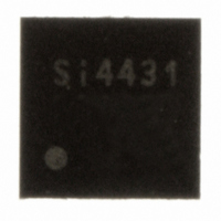
SI4431-A0-FM Silicon Laboratories Inc, SI4431-A0-FM Datasheet - Page 41

SI4431-A0-FM
Manufacturer Part Number
SI4431-A0-FM
Description
IC TXRX ISM 930MHZ 3.6V 20-QFN
Manufacturer
Silicon Laboratories Inc
Specifications of SI4431-A0-FM
Package / Case
20-QFN
Mfg Application Notes
Transitioning SI4430/31 to Rev B
Frequency
240MHz ~ 930MHz
Data Rate - Maximum
128kbps
Modulation Or Protocol
FSK, GFSK, OOK
Power - Output
13dBm
Sensitivity
-118dBm
Voltage - Supply
1.8 V ~ 3.6 V
Current - Receiving
18.5mA
Current - Transmitting
28mA
Data Interface
PCB, Surface Mount
Antenna Connector
PCB, Surface Mount
Operating Temperature
-40°C ~ 85°C
Number Of Receivers
2
Number Of Transmitters
1
Wireless Frequency
240 MHz to 930 MHz
Output Power
13 dBm
Operating Supply Voltage
1.8 V to 3.6 V
Maximum Operating Temperature
+ 85 C
Mounting Style
SMD/SMT
Maximum Supply Current
28 mA
Minimum Operating Temperature
- 40 C
Modulation
FSK, GFSK, OOK
Lead Free Status / RoHS Status
Lead free / RoHS Compliant
Applications
-
Memory Size
-
Lead Free Status / RoHS Status
Lead free / RoHS Compliant, Lead free / RoHS Compliant
Other names
336-1633-5
Available stocks
Company
Part Number
Manufacturer
Quantity
Price
Company:
Part Number:
SI4431-A0-FMR
Manufacturer:
SILICON
Quantity:
3 500
Part Number:
SI4431-A0-FMR
Manufacturer:
SILICONLABS/èٹ¯ç§‘
Quantity:
20 000
5.8. Crystal Oscillator
The Si4431 includes an integrated 30 MHz crystal oscillator with a fast start-up time of less than 600 µs when a
suitable parallel resonant crystal is used. The design is differential with the required crystal load capacitance
integrated on-chip to minimize the number of external components. By default, all that is required off-chip is the
30 MHz crystal blank.
The crystal load capacitance can be digitally programmed to accommodate crystals with various load capacitance
requirements and to slightly adjust the frequency of the crystal oscillator. The tuning of the crystal load capacitance
is programmed through the xlc[6:0] field of "Register 09h. 30 MHz Crystal Oscillator Load Capacitance". The total
internal capacitance is 12.5 pF and is adjustable in approximately 127 steps (97fF/step). The xtalshift bit is a
course shift in frequency but is not binary with xlc[6:0].
The crystal load capacitance can be digitally programmed to accommodate crystals with various load capacitance
requirements and to slightly adjust the frequency of the crystal oscillator. This latter function can be used to
compensate for crystal production tolerances. Utilizing the on-chip temperature sensor and suitable control
software even the temperature dependency of the crystal can be canceled.
The crystal load capacitance is programmed using register 09h. The typical value of the total on-chip (internal)
capacitance Cint can be calculated as follows:
Cint = 1.8 pF + 0.085 pF x xlc[6:0] + 3.7 pF x xtalshift
Note that the course shift bit xtalshift is not binary with xlc[6:0]. The total load capacitance Cload seen by the crystal
can be calculated by adding the sum of all external parasitic PCB capacitances Cext to Cint. If the maximum value
of Cint (16.3 pF) is not sufficient, an external capacitor can be added for exact tuning. See more on this,
calculating Cext and crystal selection guidelines in "11. Application Notes" on page 78.
If AFC is disabled then the synthesizer frequency may be further adjusted by programming the Frequency Offset
field fo[9:0]in "Register 73h. Frequency Offset 1" and "Register 74h. Frequency Offset 2", as discussed in "3.6.
Frequency Control" on page 27.
The crystal oscillator frequency is divided down internally and may be output to the microcontroller through one of
the GPIO pins for use as the System Clock. In this fashion, only one crystal oscillator is required for the entire
system and the BOM cost is reduced. The available clock frequencies (i.e., internal division ratios) and the GPIO
configuration are discussed further in "8.2. Microcontroller Clock" on page 56.
The Si4431 may also be driven with an external 30 MHz clock signal through the XIN pin.
5.9. Regulators
There are a total of six regulators integrated onto the Si4431. With the exception of the IF and Digital all regulators
are designed to operate with only internal decoupling. The IF and Digital regulators both require an external 1 µF
decoupling capacitor. All of the regulators are designed to operate with an input supply voltage from +1.8 to +3.6 V,
and produce a nominal regulated output voltage of +1.7 V ±5%. The internal circuitry nominally operates from this
regulated +1.7 V supply. The output stage of the of PA is not connected internally to a regulator and is connected
directly to the battery voltage.
A supply voltage should only be connected to the VDD pins. No voltage should be forced on the IF or DIG regulator
outputs.
Add R/W Function/Description
09
R/W
Crystal Oscillator Load
Capacitance
xtalshift
D7
Preliminary Rev. 0.4
xlc[6]
D6
xlc[5]
D5
xlc[4]
D4
xlc[3]
D3
xlc[2]
D2
xlc[1]
D1
xlc[0]
Si4431
D0
POR Def.
40h
41


