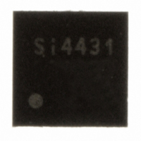
SI4431-A0-FM Silicon Laboratories Inc, SI4431-A0-FM Datasheet - Page 18

SI4431-A0-FM
Manufacturer Part Number
SI4431-A0-FM
Description
IC TXRX ISM 930MHZ 3.6V 20-QFN
Manufacturer
Silicon Laboratories Inc
Specifications of SI4431-A0-FM
Package / Case
20-QFN
Mfg Application Notes
Transitioning SI4430/31 to Rev B
Frequency
240MHz ~ 930MHz
Data Rate - Maximum
128kbps
Modulation Or Protocol
FSK, GFSK, OOK
Power - Output
13dBm
Sensitivity
-118dBm
Voltage - Supply
1.8 V ~ 3.6 V
Current - Receiving
18.5mA
Current - Transmitting
28mA
Data Interface
PCB, Surface Mount
Antenna Connector
PCB, Surface Mount
Operating Temperature
-40°C ~ 85°C
Number Of Receivers
2
Number Of Transmitters
1
Wireless Frequency
240 MHz to 930 MHz
Output Power
13 dBm
Operating Supply Voltage
1.8 V to 3.6 V
Maximum Operating Temperature
+ 85 C
Mounting Style
SMD/SMT
Maximum Supply Current
28 mA
Minimum Operating Temperature
- 40 C
Modulation
FSK, GFSK, OOK
Lead Free Status / RoHS Status
Lead free / RoHS Compliant
Applications
-
Memory Size
-
Lead Free Status / RoHS Status
Lead free / RoHS Compliant, Lead free / RoHS Compliant
Other names
336-1633-5
Available stocks
Company
Part Number
Manufacturer
Quantity
Price
Company:
Part Number:
SI4431-A0-FMR
Manufacturer:
SILICON
Quantity:
3 500
Part Number:
SI4431-A0-FMR
Manufacturer:
SILICONLABS/èٹ¯ç§‘
Quantity:
20 000
Si4431
2.1. Operating Modes
The Si4431 provides several modes of operation which can be used to optimize the power consumption of the
device application. Depending upon the system communication protocol, the optimal trade-off between the radio
wake time and power consumption can be achieved.
Table 9 summarizes the modes of operation of the Si4431. In general, any given mode of operation may be
classified as an Active mode or a Power Saving mode. The table indicates which block(s) are enabled (active) in
each corresponding mode. With the exception the Shutdown mode, all can be dynamically selected by sending the
appropriate commands over the SPI in order to optimize the average current consumption. An “X” in any cell
means that, in the given mode of operation, that block can be independently programmed to be either ON or OFF,
without noticeably affecting the current consumption. The SPI circuit block includes the SPI interface and the
register space. The 32 kHz OSC circuit block includes the 32.768 kHz RC oscillator or 32.768 kHz crystal
oscillator, and wake-up timer. AUX (Auxiliary Blocks) includes the temperature sensor, general purpose ADC, and
low-battery detector.
18
*Note: 28 mA at +13 dBm.
Shutdown
Transmit
Standby
Receive
Sensor
Tuning
Ready
Name
Mode
Sleep
OFF (Register
contents lost)
ON (Register
Digital LDO
retained)
contents
OFF
SPI
ON
ON
ON
ON
ON
ON
ON
32 kHz OSC
Table 9. Operating Modes
OFF
OFF
ON
X
X
X
X
X
Preliminary Rev. 0.4
Circuit Blocks
AUX
OFF
OFF
ON
X
X
X
X
X
30 MHz
XTAL
OFF
OFF
OFF
OFF
ON
ON
ON
ON
OFF
OFF
OFF
OFF
OFF
PLL
ON
ON
ON
OFF
OFF
OFF
OFF
OFF
OFF
OFF
ON
PA
OFF
OFF
OFF
OFF
OFF
OFF
OFF
ON
RX
18.5 mA
600 µA
28 mA*
400 nA
800 nA
9.5 mA
10 nA
1 µA
I
VDD


