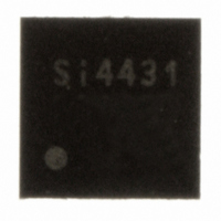
SI4431-A0-FM Silicon Laboratories Inc, SI4431-A0-FM Datasheet - Page 57

SI4431-A0-FM
Manufacturer Part Number
SI4431-A0-FM
Description
IC TXRX ISM 930MHZ 3.6V 20-QFN
Manufacturer
Silicon Laboratories Inc
Specifications of SI4431-A0-FM
Package / Case
20-QFN
Mfg Application Notes
Transitioning SI4430/31 to Rev B
Frequency
240MHz ~ 930MHz
Data Rate - Maximum
128kbps
Modulation Or Protocol
FSK, GFSK, OOK
Power - Output
13dBm
Sensitivity
-118dBm
Voltage - Supply
1.8 V ~ 3.6 V
Current - Receiving
18.5mA
Current - Transmitting
28mA
Data Interface
PCB, Surface Mount
Antenna Connector
PCB, Surface Mount
Operating Temperature
-40°C ~ 85°C
Number Of Receivers
2
Number Of Transmitters
1
Wireless Frequency
240 MHz to 930 MHz
Output Power
13 dBm
Operating Supply Voltage
1.8 V to 3.6 V
Maximum Operating Temperature
+ 85 C
Mounting Style
SMD/SMT
Maximum Supply Current
28 mA
Minimum Operating Temperature
- 40 C
Modulation
FSK, GFSK, OOK
Lead Free Status / RoHS Status
Lead free / RoHS Compliant
Applications
-
Memory Size
-
Lead Free Status / RoHS Status
Lead free / RoHS Compliant, Lead free / RoHS Compliant
Other names
336-1633-5
Available stocks
Company
Part Number
Manufacturer
Quantity
Price
Company:
Part Number:
SI4431-A0-FMR
Manufacturer:
SILICON
Quantity:
3 500
Part Number:
SI4431-A0-FMR
Manufacturer:
SILICONLABS/èٹ¯ç§‘
Quantity:
20 000
8.3. General Purpose ADC
An 8-bit SAR ADC is integrated onto the chip for general purpose use, as well as for digitizing the temperature
sensor reading. “Register 0Fh. ADC Configuration,” on page 99 must be configured depending on the use of the
GP ADC before use. The architecture of the ADC is demonstrated in Figure 24. First the input of the ADC must be
selected by setting the ADCSEL[2:0] depending on the use of the ADC. For instance, if the ADC is going to be
used to read out the internal temperature sensor, then ADCSEL[2:0] should be set to 000. Next, the input reference
voltage to the ADC must be chosen. By default, the ADC uses the bandgap voltage as a reference so the input
range of the ADC is from 0–1.02 V with an LSB resolution of 4 mV (1.02/255). Changing the ADC reference will
change the LSB resolution accordingly.
Every time the ADC conversion is desired, the ADCStart bit in “Register 0Fh. ADC Configuration,” on page 99 must
be set to 1. This is a self clearing bit that will be cleared at the end of the conversion cycle of the ADC. The
conversion time for the ADC is 350 us. After the 350 us or when the ADCstart/busy bit is cleared, then the ADC
value may be read out of "Register 11h. ADC Value". Setting the "Register 10h. ADC Sensor Amplifier Offset", ADC
Sensor Amplifier Offset is only necessary when the ADC is configured to used as a Bridge Sensor as described in
the following section.
Add R/W
0F
10
11
R/W
R/W
R
ADC Sensor Amplifier Offset
Function/Description
ADC Configuration
ADC Value
GPIO0
GPIO1
GPIO2
TS
V
BG
(1.2V)
ADCSEL<2:0>
Figure 24. General Purpose ADC Architecture
Diff. MUX
adcstart/adcbusy
adc[7]
OTR<3:0>
D7
V
V
BAT
BAT
Diff. Amp.
/ 3
/ 2
GAIN<1:0>
adcsel[2] adcsel[1] adcsel[0]
Preliminary Rev. 0.4
adc[6]
D6
ADCSEL<2:0>
Input MUX
REFSEL<1:0>
adc[5]
Ref MUX
D5
adc[4]
D4
Vin
Vref
adcoffs[3]
adcref[1]
0-1020mV / 0-255
adc[3]
8-bit ADC
D3
adcoffs[2]
adcref[0]
adc[2]
D2
VMEAS<7:0>
adcgain[1] adcgain[0]
adcoffs[1]
adc[1]
D1
adcoffs[0]
adc[0]
Si4431
D0
POR Def.
00h
00h
—
57


