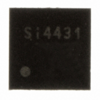
SI4431-A0-FM Silicon Laboratories Inc, SI4431-A0-FM Datasheet - Page 40

SI4431-A0-FM
Manufacturer Part Number
SI4431-A0-FM
Description
IC TXRX ISM 930MHZ 3.6V 20-QFN
Manufacturer
Silicon Laboratories Inc
Specifications of SI4431-A0-FM
Package / Case
20-QFN
Mfg Application Notes
Transitioning SI4430/31 to Rev B
Frequency
240MHz ~ 930MHz
Data Rate - Maximum
128kbps
Modulation Or Protocol
FSK, GFSK, OOK
Power - Output
13dBm
Sensitivity
-118dBm
Voltage - Supply
1.8 V ~ 3.6 V
Current - Receiving
18.5mA
Current - Transmitting
28mA
Data Interface
PCB, Surface Mount
Antenna Connector
PCB, Surface Mount
Operating Temperature
-40°C ~ 85°C
Number Of Receivers
2
Number Of Transmitters
1
Wireless Frequency
240 MHz to 930 MHz
Output Power
13 dBm
Operating Supply Voltage
1.8 V to 3.6 V
Maximum Operating Temperature
+ 85 C
Mounting Style
SMD/SMT
Maximum Supply Current
28 mA
Minimum Operating Temperature
- 40 C
Modulation
FSK, GFSK, OOK
Lead Free Status / RoHS Status
Lead free / RoHS Compliant
Applications
-
Memory Size
-
Lead Free Status / RoHS Status
Lead free / RoHS Compliant, Lead free / RoHS Compliant
Other names
336-1633-5
Available stocks
Company
Part Number
Manufacturer
Quantity
Price
Company:
Part Number:
SI4431-A0-FMR
Manufacturer:
SILICON
Quantity:
3 500
Part Number:
SI4431-A0-FMR
Manufacturer:
SILICONLABS/èٹ¯ç§‘
Quantity:
20 000
Si4431
The reference frequency to the PLL is 10 MHz. The PLL utilizes a differential L-C VCO, with integrated on-chip
spiral inductors. The output of the VCO is followed by a configurable divider which will divide down the signal to the
desired output frequency band. The modulus of this divider stage is controlled dynamically by the output from the
- modulator. The tuning resolution of the - modulator is determined largely by the over-sampling rate and the
number of bits carried internally. The tuning resolution is sufficient to tune to the commanded frequency with a
maximum accuracy of 312.5 Hz anywhere in the range between 240–930 MHz.
5.6.1. VCO
The output of the VCO is automatically divided down to the correct output frequency depending on the hbsel and
fb[4:0] fields in "Register 75h. Frequency Band Select". A 2X VCO is utilized to help avoid problems due to
frequency pulling, especially when turning on the integrated Power Amplifier. In receive mode, the LO frequency is
automatically shifted downwards (without reprogramming) by the IF frequency of 937.5 kHz, allowing transmit and
receive operation on the same frequency. The VCO integrates the resonator inductor, tuning varactor, so no
external VCO components are required.
The VCO uses capacitance bank to cover the wide frequency range specified. The capacitance bank will
automatically be calibrated every time the synthesizer is enabled. In certain fast hopping applications this might not
be desirable so the VCO calibration may be skipped by setting the appropriate register.
5.7. Power Amplifier
The Si4431 contains an internal integrated power amplifier (PA) capable of transmitting at output levels between –8
to +13 dBm. The output power is programmable in 3 dB steps through the txpow[2:0] field in "Register 6Dh. TX
Power".
The PA design is single-ended and is implemented as a two stage class CE amplifier with efficiency in the range of
45–50% while transmitting at maximum power. The efficiency drops to approximately 20% when operating at the
lowest power steps. Due to the high efficiency a simple filter is required on the board to filter the harmonics. The PA
output is ramped up and down to prevent unwanted spectral splatter.
5.7.1. Output Power Selection
The output power is configurable in 3 dB steps from –8 to +13 dBm with the txpow[2:0] field in "Register 6Dh. TX
Power". The PA output is ramped up and down to prevent unwanted spectral splatter.
Extra output power can allow use of a cheaper smaller antenna, greatly reducing the overall BOM cost. The higher
power setting of the chip achieves maximum possible range, but of course comes at the cost of higher TX current
consumption. However, depending on the duty cycle of the system, the effect on battery life may be insignificant.
Contact Silicon Labs Support for help in evaluating this tradeoff.
40
Add R/W Function/Description
6D
R/W
TX Power
D7
txpow[2:0]
000
001
010
011
100
101
110
111
D6
Preliminary Rev. 0.4
D5
Output Power
D4
+10 dBm
+13 dBm
+1 dBm
+4 dBm
+7 dBm
–8 dBm
–5 dBm
–2 dBm
D3
txpow[2]
D2
txpow[1]
D1
txpow[0]
D0
POR Def.
07h


