IPR-HPMCII Altera, IPR-HPMCII Datasheet
IPR-HPMCII
Specifications of IPR-HPMCII


Related parts for IPR-HPMCII


IPR-HPMCII Summary of contents
Page 1
... DDR3 SDRAM Controller with ALTMEMPHY IP User Guide External Memory Interface Handbook Volume 3 Section II. DDR3 SDRAM Controller with ALTMEMPHY IP 101 Innovation Drive San Jose, CA 95134 www.altera.com EMI_DDR3_UG-2.1 Document last updated for Altera Complete Design Suite version: Document publication date: User Guide 10.1 December 2010 Subscribe ...
Page 2
... Altera warrants performance of its semiconductor products to current specifications in accordance with Altera’s standard warranty, but reserves the right to make changes to any products and services at any time without notice. Altera assumes no responsibility or liability arising out of the application or use of any information, product, or service described herein except as expressly agreed to in writing by Altera. Altera customers are advised to obtain the latest version of device specifications before relying on any published information and before placing orders for products or services ...
Page 3
... Chapter 5. Functional Description—ALTMEMPHY Block Description . . . . . . . . . . . . . . . . . . . . . . . . . . . . . . . . . . . . . . . . . . . . . . . . . . . . . . . . . . . . . . . . . . . . . . . 5–2 Calibration . . . . . . . . . . . . . . . . . . . . . . . . . . . . . . . . . . . . . . . . . . . . . . . . . . . . . . . . . . . . . . . . . . . . . . . . . . . 5–3 DDR3 SDRAM Without Leveling . . . . . . . . . . . . . . . . . . . . . . . . . . . . . . . . . . . . . . . . . . . . . . . . . . . . . 5–3 Step 1: Memory Device Initialization . . . . . . . . . . . . . . . . . . . . . . . . . . . . . . . . . . . . . . . . . . . . . . . . . . 5–4 Step 2: Write Training Patterns . . . . . . . . . . . . . . . . . . . . . . . . . . . . . . . . . . . . . . . . . . . . . . . . . . . . . . . 5–4 December 2010 Altera Corporation External Memory Interface Handbook Volume 3 Section II. DDR3 SDRAM Controller with ALTMEMPHY IP User Guide Contents ...
Page 4
... Timer Logic . . . . . . . . . . . . . . . . . . . . . . . . . . . . . . . . . . . . . . . . . . . . . . . . . . . . . . . . . . . . . . . . . . . . . . . . . . 6–3 Initialization State Machine . . . . . . . . . . . . . . . . . . . . . . . . . . . . . . . . . . . . . . . . . . . . . . . . . . . . . . . . . . . . . 6–3 Address and Command Decode . . . . . . . . . . . . . . . . . . . . . . . . . . . . . . . . . . . . . . . . . . . . . . . . . . . . . . . . 6–3 PHY Interface Logic . . . . . . . . . . . . . . . . . . . . . . . . . . . . . . . . . . . . . . . . . . . . . . . . . . . . . . . . . . . . . . . . . . . 6–4 ODT Generation Logic . . . . . . . . . . . . . . . . . . . . . . . . . . . . . . . . . . . . . . . . . . . . . . . . . . . . . . . . . . . . . . . . . 6–4 Low-Power Mode Logic . . . . . . . . . . . . . . . . . . . . . . . . . . . . . . . . . . . . . . . . . . . . . . . . . . . . . . . . . . . . . . . 6–4 External Memory Interface Handbook Volume 3 Section II. DDR3 SDRAM Controller with ALTMEMPHY IP User Guide Contents December 2010 Altera Corporation ...
Page 5
... Half Rate Write for Native Interface . . . . . . . . . . . . . . . . . . . . . . . . . . . . . . . . . . . . . . . . . . . . . . . . . . . . . 9–8 Initialization Timing . . . . . . . . . . . . . . . . . . . . . . . . . . . . . . . . . . . . . . . . . . . . . . . . . . . . . . . . . . . . . . . . . . 9–10 Calibration Timing . . . . . . . . . . . . . . . . . . . . . . . . . . . . . . . . . . . . . . . . . . . . . . . . . . . . . . . . . . . . . . . . . . . 9–12 DDR3 High-Performance Controllers 9–13 Half-Rate Read (Burst-Aligned Address 9–14 Half-Rate Write (Burst-Aligned Address 9–16 December 2010 Altera Corporation External Memory Interface Handbook Volume 3 Section II. DDR3 SDRAM Controller with ALTMEMPHY IP User Guide v ...
Page 6
... Half-Rate Write With Gaps . . . . . . . . . . . . . . . . . . . . . . . . . . . . . . . . . . . . . . . . . . . . . . . . . . . . . . . . . . . . 9–23 Half-Rate Write Operation (Merging Writes 9–24 Write-Read-Write-Read Operation . . . . . . . . . . . . . . . . . . . . . . . . . . . . . . . . . . . . . . . . . . . . . . . . . . . . . 9–26 Additional Information Document Revision History . . . . . . . . . . . . . . . . . . . . . . . . . . . . . . . . . . . . . . . . . . . . . . . . . . . . . . . . . . . Info–1 How to Contact Altera . . . . . . . . . . . . . . . . . . . . . . . . . . . . . . . . . . . . . . . . . . . . . . . . . . . . . . . . . . . . . . . . Info–1 Typographic Conventions . . . . . . . . . . . . . . . . . . . . . . . . . . . . . . . . . . . . . . . . . . . . . . . . . . . . . . . . . . . . . Info–2 External Memory Interface Handbook Volume 3 Section II. DDR3 SDRAM Controller with ALTMEMPHY IP User Guide Contents ...
Page 7
... The DDR3 SDRAM Controller with ALTMEMPHY IP works in conjunction with the Altera ALTMEMPHY megafunction. The DDR3 SDRAM Controller with ALTMEMPHY IP and ALTMEMPHY megafunction support DDR3 SDRAM interfaces in half-rate mode. The DDR3 SDRAM Controller with ALTMEMPHY IP offers two controller architectures: the high-performance controller (HPC) and the high-performance controller II (HPC II) ...
Page 8
... Quartus II version, refer to the Quartus II Software Release Device Family Support The MegaCore function provides either final or preliminary support for target Altera device families: ■ Final support means the core is verified with final timing models for this device family ...
Page 9
... III Stratix IV Other device families Features The ALTMEMPHY megafunction offers the following features: ■ Simple setup. Support for the Altera PHY Interface (AFI) for DDR3 SDRAM on all supported ■ devices. ■ Automated initial calibration eliminating complicated read data timing calculations. ■ ...
Page 10
... DDR3 SDRAM HPC and mitigation RC Chapter 1: About This IP Features Controller Architecture HPC HPC — v — v — (1) v — v — v — v — v — v — (2) v — — v — v — — v — — v — — December 2010 Altera Corporation ...
Page 11
... Chapter 1: About This IP Unsupported Features Table 1–3. DDR3 SDRAM HPC and HPC II Features (Part Features IP functional simulation models for use in Altera-supported VHDL and Verilog HDL simulator Notes to Table 1–3: (1) HPC II supports additive latency values greater or equal to t (2) This feature is not supported with DDR3 SDRAM with leveling ...
Page 12
... ALUTs 1,189 2 18 1,264 4 2 1,970 12 22 2,038 13 2 M9K Memory Blocks ALUTs 1,047 1 40 1,196 1 80 2,080 1 320 2,228 1 360 2,723 2 80 3,235 2 160 6,487 5 640 6,984 5 720 2,867 2 80 3,391 2 160 6,645 5 640 7,144 5 720 December 2010 Altera Corporation ...
Page 13
... Local Data Width (Bits 256 288 Table 1–9. Resource Utilization in Stratix III Devices Local Data Width (Bits 256 288 December 2010 Altera Corporation Table 1–7 show the typical sizes for the DDR3 SDRAM HPC (including Memory Width Combinational (Bits) ALUTs 8 1,891 16 1,966 64 2,349 ...
Page 14
... Figure 1–2. Directory Structure You need a license for the MegaCore function only when you are completely satisfied with its functionality and performance, and want to take your design to production. To use the DDR3 SDRAM HPC, you can request a license file from the Altera web site at www.altera.com/licensing license file, Altera emails you a license ...
Page 15
... Chapter 1: About This IP Installation and Licensing Free Evaluation Altera's OpenCore Plus evaluation feature is only applicable to the DDR3 SDRAM HPC. With the OpenCore Plus evaluation feature, you can perform the following actions: ■ Simulate the behavior of a megafunction (Altera MegaCore function or AMPP megafunction) within your system. ■ ...
Page 16
... External Memory Interface Handbook Volume 3 Section II. DDR3 SDRAM Controller with ALTMEMPHY IP User Guide Chapter 1: About This IP Installation and Licensing December 2010 Altera Corporation ...
Page 17
... You can only instantiate the ALTMEMPHY megafunction using the MegaWizard Plug-In Manager flow. Figure 2–1 shows the stages for creating a system in the Quartus II software using either one of the flows. Figure 2–1. Design Flow December 2010 Altera Corporation Select Design Flow SOPC Builder Flow Specify Parameters Complete ...
Page 18
... For detailed explanation of the parameters, refer to the Settings” on page External Memory Interface Handbook Volume 3 Section II. DDR3 SDRAM Controller with ALTMEMPHY IP User Guide ® II processor and volume 4 section in volume 6 of the External Memory 3–1. December 2010 Altera Corporation Chapter 2: Getting Started SOPC Builder Flow of the Quartus II “Parameter ...
Page 19
... If there are warnings about overlapping addresses, on the System menu, click Auto Assign Base Addresses. If you enable ECC and there are warnings about overlapping IRQs, on the System menu click Auto Assign IRQs. December 2010 Altera Corporation Table 2–1 for more Avalon-MM addresses. Reset Vector Offset ...
Page 20
... An IP functional simulation model is a cycle-accurate VHDL or Verilog HDL model produced by the Quartus II software. External Memory Interface Handbook Volume 3 Section II. DDR3 SDRAM Controller with ALTMEMPHY IP User Guide MegaWizard Plug-In Manager Flow “Compiling and Simulating” on page 3–1. December 2010 Altera Corporation Chapter 2: Getting Started 4–1. “Parameter ...
Page 21
... On the File menu, click Open. b. Browse to <variation name>_example_top and click Open the Project menu, click Set as Top-Level Entity. December 2010 Altera Corporation External Memory Interface Handbook Volume 3 Section II. DDR3 SDRAM Controller with ALTMEMPHY IP User Guide 2–5 ...
Page 22
... A wrapper file, for compilation only, that calls the sequencer file, created based on the language you chose in the MegaWizard Plug-In Manager. A wrapper file, for simulation only, that calls the sequencer file, created based on the language you chose in the MegaWizard Plug-In Manager. December 2010 Altera Corporation Generated Files ...
Page 23
... December 2010 Altera Corporation Contains all modules of the ALTMEMPHY variation except for the sequencer. This file is always in Verilog HDL language regardless of the language you chose in the MegaWizard Plug-In Manager. The DDR3 SDRAM sequencer is included in the < ...
Page 24
... ALTMEMPHY variation. If your top-level design pin names do not match the default pin names or a prefixed version, edit the assignments in this file. Chapter 2: Getting Started Generated Files Description 2–6, the MegaWizard also generates Description December 2010 Altera Corporation ...
Page 25
... December 2010 Altera Corporation Description VHDL or Verilog HDL IP functional simulation model. ECC functional simulation model. Description A controller wrapper that instantiates the alt_ddrx_controller.v file and configures the controller accordingly by the wizard. Decodes the state machine outputs into the memory address and command signals ...
Page 26
... MEM_IF_CLK_PS_STR MEM_IF_MR_0 External Memory Interface Handbook Volume 3 Section II. DDR3 SDRAM Controller with ALTMEMPHY IP User Guide Table 2–7 Parameter HIGH 10 6 DELAY_CHAIN2 7200 2 3300 3300 ps 4641 Chapter 2: Getting Started HardCopy Device Migration Guidelines shows the key parameters. Setting December 2010 Altera Corporation ...
Page 27
... FPGA speed grade. Table 2–9. Post-fit PLL Parameters When Using a HardCopy Device VCO OPERATING FREQUENCY VCO PHASE SHIFT STEP MEMORY CLOCK PERIOD PLL PHASE STEPS PER MEMCLK PERIOD December 2010 Altera Corporation Parameter 40 240 Parameter 1515 MHz 82 ps ...
Page 28
... Quartus II Fitter restricts the VCO operating range to Table in the HardCopy III Device Handbook, Volume 1, and in the HardCopy IV Device Handbook, Volume 1. Chapter 2: Getting Started HardCopy Device Migration Guidelines 2–8. This restriction produces a phase HardCopy III Device HardCopy IV Device December 2010 Altera Corporation ...
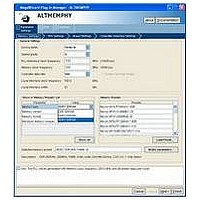
Page 29
... The Finish button is disabled until you correct all the errors indicated in this window. December 2010 Altera Corporation 3. Parameter Settings External Memory Interface Handbook Volume 3 Section II. DDR3 SDRAM Controller with ALTMEMPHY IP User Guide (Figure 3– ...
Page 30
... PHY sequencer settings match. The compilation of the design can be executed in the faster speed grade. External Memory Interface Handbook Volume 3 Section II. DDR3 SDRAM Controller with ALTMEMPHY IP User Guide Chapter 3: Parameter Settings ALTMEMPHY Parameter Settings Figure 3–1. If you cannot find the Description Table 1–2 on page 1–3 shows supported device December 2010 Altera Corporation ...
Page 31
... If you save the new settings in a directory other than the default directory, click Load Preset in the Memory Settings tab to load the settings into the Memory Presets list. December 2010 Altera Corporation Description External Memory Interface Handbook Volume 3 Section II. DDR3 SDRAM Controller with ALTMEMPHY IP User Guide ...
Page 32
... The Advanced option is only available for Arria II GX and Stratix IV devices. This option shows the percentage of memory specification that is calibrated by the FPGA. The percentage values are estimated by Altera based on the process variation. External Memory Interface Handbook Volume 3 Section II. DDR3 SDRAM Controller with ALTMEMPHY IP User Guide ...
Page 33
... Memory format Unbuffered See the memory Maximum memory frequency device datasheet Column address width December 2010 Altera Corporation Table 3–5 describe the DDR3 SDRAM parameters available for (1) Units Defines the number of differential clock pairs driven from the FPGA to the memory. Memory clock pins use the signal splitter feature in Arria II GX, Stratix III, and Stratix IV devices for differential signaling ...
Page 34
... Specifies whether you are using DM pins for write — operation. Altera devices do not support DM pins with ×4 mode. Specifies the frequency limits from the memory data sheet per given CAS latency. The ALTMEMPHY MegaWizard Plug-In Manager generates a warning if the ...
Page 35
... This option is not supported by the DDR3 SDRAM Controller with ALTMEMPHY IP, so set to Full Array if you are using the Altera controller. 111}, Section II. DDR3 SDRAM Controller with ALTMEMPHY IP User Guide 3–7 ...
Page 36
... Determines the temperature range for self refresh. You need to also use the optional auto self refresh option — when using this option. The Altera controller currently does not support the extended temperature self-refresh operation. (Note 1) ...
Page 37
... IS t 0–700 QHS t 0.1–0.6 QH December 2010 Altera Corporation (Note 1) Range Units Minimum write-to-read command delay. The controller waits for this period of time after the end of a write command before issuing a subsequent read command the same bank. This timing parameter is specified in clock cycles and the value is rounded off to the next integer ...
Page 38
... Derating Memory Setup and Hold Timing Because the base setup and hold time specifications from the memory device datasheet assume input slew rates that may not be true for Altera devices, derate and update the following memory device specifications in the Preset Editor dialog box: t ■ ...
Page 39
... DH REF 310 ps PHY Settings Click Next or the PHY Settings tab to set the options described in options are available if they apply to the target Altera device. Table 3–6. ALTMEMPHY PHY Settings (Part Parameter Name Applicable Device Families Use dedicated PLL HardCopy II and Stratix II ...
Page 40
... This parameter generates the timing constraints in the .sdc file. Choose between Full Calibration (long simulation time), Quick Calibration, or Skip Calibration. For more information, refer to the Simulation the External Memory Interface Handbook. December 2010 Altera Corporation Chapter 3: Parameter Settings ALTMEMPHY Parameter Settings External Memory section in volume 4 of ...
Page 41
... Memory Settings ■ PHY Settings ■ Board Settings ■ Controller Settings December 2010 Altera Corporation Units — Sets the single-rank or multi-rank configuration. V/ns Sets the differential slew rate for the CK and CK# signals. V/ns Sets the slew rate for the address and command signals. ...
Page 42
... Controller Settings tab. External Memory Interface Handbook Volume 3 Section II. DDR3 SDRAM Controller with ALTMEMPHY IP User Guide DDR3 SDRAM Controller with ALTMEMPHY Parameter Settings Settings, PHY Settings, and Board Settings Chapter 3: Parameter Settings tabs provide the same December 2010 Altera Corporation ...
Page 43
... Enable auto-precharge control Local-to-memory address mapping Command queue look-ahead depth December 2010 Altera Corporation — Specifies the controller architecture. Turn on to enable the controller to allow you to have control on when to place the external memory device in self-refresh mode, Both refer to “User-Controlled Self-Refresh Logic” on page 7–8 (HPC II) ...
Page 44
... Command Queue Look-Ahead Depth option. Refer to Management Logic” on page 7–4 Chapter 3: Parameter Settings Description “Error for HPC, and “Error for HPC II. “Error 7–7. “Bank Management Logic” on page 7–4 “Bank for more information. December 2010 Altera Corporation ...
Page 45
... Controller Architecture Multiple controller clock sharing Local interface protocol December 2010 Altera Corporation This option is only available in SOPC Builder Flow. Turn on to allow one controller to use the Avalon clock from another controller in the system that has a compatible PLL. This option Both ...
Page 46
... External Memory Interface Handbook Volume 3 Section II. DDR3 SDRAM Controller with ALTMEMPHY IP User Guide Chapter 3: Parameter Settings DDR3 SDRAM Controller with ALTMEMPHY Parameter Settings December 2010 Altera Corporation ...
Page 47
... I/O standard, pin location, and other assignments, such as termination and drive strength settings. Some of these tasks are listed in the ALTMEMPHY Generation window. For most systems, Altera recommends that you use the Advanced I/O Timing feature by using the Board Trace Model command in the Quartus II software to set the termination and output pin loads for the device ...
Page 48
... Tcl script you should change set single_bit {[0]} to set single_bit {}. or External Memory Interface Handbook Volume 3 Section II. DDR3 SDRAM Controller with ALTMEMPHY IP User Guide Chapter 4: Compiling and Simulating <your instance name> December 2010 Altera Corporation Compiling the Design ...
Page 49
... Device & Pin Options dialog box. If you are using any other device and not using advanced I/O timing, specify the output pin loading for all memory interface pins. December 2010 Altera Corporation External Memory Interface Handbook Volume 3 Section II. DDR3 SDRAM Controller with ALTMEMPHY IP User Guide ...
Page 50
... Simulating the Design During system generation, SOPC Builder optionally generates a simulation model and testbench for the entire system, which you can use to easily simulate your system in any of Altera's supported simulation tools. The MegaWizard also generates a set of ® ModelSim functional simulation models, and plain-text RTL design files that describe your ...
Page 51
... Full Calibration. You must use a memory-vendor provided memory model that supports write leveling calibration you are simulating your ALTMEMPHY-based design with a Denali model, Altera recommends that you use full calibration mode. f For more information about simulation, refer to the the External Memory Interface Handbook ...
Page 52
... External Memory Interface Handbook Volume 3 Section II. DDR3 SDRAM Controller with ALTMEMPHY IP User Guide Chapter 4: Compiling and Simulating Simulating the Design December 2010 Altera Corporation ...
Page 53
... The ALTMEMPHY megafunction creates the datapath between the memory device and the memory controller, and user logic in various Altera devices. The ALTMEMPHY megafunction GUI helps you configure multiple variations of a memory interface. You can then connect the ALTMEMPHY megafunction variation with either a user-designed controller or with an Altera high-performance controller. ...
Page 54
... Chapter 5: Functional Description—ALTMEMPHY shows the major blocks of the ALTMEMPHY megafunction FPGA ALTMEMPHY Write Datapath Address and Command Memory Datapath Controller External Memory Clock Device and Reset Management DLL PLL Read Datapath Sequencer Block Description User Logic December 2010 Altera Corporation ...
Page 55
... Block Description The major advantage of the ALTMEMPHY megafunction is that it supports an initial calibration sequence to remove process variations in both the Altera device and the memory device. In Arria series and Stratix series devices, the DDR3 SDRAM ALTMEMPHY calibration process centers the resynchronization clock phase into the middle of the captured data valid window to maximize the resynchronization setup and hold margin ...
Page 56
... Memory Device and PHY Initialization Write Training Patterns Read Resynchronization Clock Phase Read and Write Datapath Timing Address and Command Clock Cycle Postamble Prepare for User Mode VT Tracking User Mode “Step 7: Prepare for User Mode”. Block Description December 2010 Altera Corporation ...
Page 57
... VT tracking is a background process that tracks the voltage and temperature variations to maintain the relationship between the resynchronization or capture clock and the data valid window that are achieved at calibration. December 2010 Altera Corporation (“Step 3: Read Resynchronization (Capture) Clock to “Step 4: Read and Write Datapath Section II. DDR3 SDRAM Controller with ALTMEMPHY IP User Guide 5– ...
Page 58
... Any change in the delay of the mimic path indicates a corresponding change in the round-trip delay, and a corresponding adjustment is made to the phase of the resynchronization or capture clock. External Memory Interface Handbook Volume 3 Section II. DDR3 SDRAM Controller with ALTMEMPHY IP User Guide Chapter 5: Functional Description—ALTMEMPHY Block Description December 2010 Altera Corporation ...
Page 59
... Therefore, the sequencer must adjust the clock to launch the DQS/DQSn and DQ signals so that it is appropriately aligned to the CK/CKn signals on each device. The DDR3 SDRAM leveling sequencer during calibration writes to the following locations: December 2010 Altera Corporation datain ddiodatain outclk mimic_data_in ...
Page 60
... The calibration assumes that the skew for all the DQS launch times is one clock period maximum. The VT tracking portion of the DDR3 SDRAM sequencer is similar to that of the DDR or DDR2 SDRAM sequencer. External Memory Interface Handbook Volume 3 Section II. DDR3 SDRAM Controller with ALTMEMPHY IP User Guide Chapter 5: Functional Description—ALTMEMPHY Block Description December 2010 Altera Corporation ...
Page 61
... ODT setting, and initializing the memory device DLL. Some of these settings may be different to those you set; however, these are changed to the correct values (at the end of calibration) in December 2010 Altera Corporation Memory Device and PHY Initialization Write Leveling ...
Page 62
... External Memory Interface Handbook Volume 3 Section II. DDR3 SDRAM Controller with ALTMEMPHY IP User Guide Chapter 5: Functional Description—ALTMEMPHY -margin register in the DDR3 SDRAM to monitor the DQSS December 2010 Altera Corporation Block Description ...
Page 63
... This scheme applies to all address and command signals, except for mem_cs_n, mem_cke, and mem_odt signals in half-rate mode. 1 Refer to Table 5–1 on page 5–14 the rest of the clocks. December 2010 Altera Corporation 5–5. 5–6. Figure 5–6). This applies to all address and command signals in to see the frequency relationship of mem_clk_2x with Section II. DDR3 SDRAM Controller with ALTMEMPHY IP User Guide 5– ...
Page 64
... Section II. DDR3 SDRAM Controller with ALTMEMPHY IP User Guide Chapter 5: Functional Description—ALTMEMPHY NOP PCH NOP ACT WR 0000 0001 0004 [1] [1] [2] [3] [3] [4] Figure 5–6 shows a NOP command followed by five back-to-back Block Description NOP 0008 000C 0010 0000 [4] [4] for illustrations of this December 2010 Altera Corporation ...
Page 65
... The PLL uses With No Compensation option to minimize jitter. Changing the PLL compensation to a different operation mode may result in inaccurate timing results. December 2010 Altera Corporation External Memory Interface Handbook Volume 3 Section II. DDR3 SDRAM Controller with ALTMEMPHY IP User Guide ...
Page 66
... This clock is for clocking DQS and as a reference clock for the memory devices. This clock is for clocking the data out of the DDR I/O (DDIO) pins in advance of the DQS strobe (or equivalent result, its phase leads that of the mem_clk_2x by 90°. December 2010 Altera Corporation ...
Page 67
... C4 resync_clk_2x C5 measure_clk_2x Note to Table 5–1: (1) The _1x clock represents a frequency that is half of the memory clock frequency; the _2x clock represents the memory clock frequency. December 2010 Altera Corporation Phase Clock Clock Rate (Degrees) Network Type –90° Full-Rate Global –90° ...
Page 68
... This clock is for VT tracking. This free-running clock measures relative phase shifts between the internal clock(s) and those being fed back through a mimic path result, you can track VT effects on the FPGA and compensate for the effects. December 2010 Altera Corporation ...
Page 69
... Q CLR CLR Another pll_ref_clk system Optional clock global_reset_n reset_ request_n edge detect and reset counter soft_reset_n December 2010 Altera Corporation Clock Phase Clock Network (Degrees) Rate Type Set in the Half-Rate Regional GUI Figure 5–9 show the main features of the reset management block for ...
Page 70
... HIGH) c0 global_or_soft_reset_n Chapter 5: Functional Description—ALTMEMPHY Block Description Internal reset signal pll_reconfig_reset_ams_n signal for the PLL clock-domain crossing registers SET Q SET CLR CLR pll_reconfig_reset_ams_n_r reset_request_n reset_master_ams global_pre_clear SET Q SET CLR CLR phy_clk_out phy_internal_reset_n PHY resets Reset Pipes December 2010 Altera Corporation ...
Page 71
... SDR and HDR clocks are generated, the read and write pointers are continuously incremented by the same PLL, and the 4n-bit wide read data follows the 2n-bit wide write data with a constant latency December 2010 Altera Corporation SDR Data Capture Data Resynchronization ...
Page 72
... DQS input signals at the end of the read postamble time do not cause erroneous data to be captured as a result of postamble glitches. External Memory Interface Handbook Volume 3 Section II. DDR3 SDRAM Controller with ALTMEMPHY IP User Guide Chapter 5: Functional Description—ALTMEMPHY Block Description December 2010 Altera Corporation ...
Page 73
... DQ input registers at the end of a read operation. This ensures that any glitches on the DQS input signals at the end of the read postamble time do not cause erroneous data to be captured as a result of postamble glitches. December 2010 Altera Corporation Read Datapath dio_rdata3_1x ...
Page 74
... External Memory Interface Handbook Volume 3 Section II. DDR3 SDRAM Controller with ALTMEMPHY IP User Guide Write Datapath wdp_wdata_h Data Multiplexing wdp_wdata_l write_clk_2x Figure 5–12 by wdp_wdata3_1x, wdp_wdata2_1x, wdp_wdata1_1x, and Chapter 5: Functional Description—ALTMEMPHY Block Description ctl_mem_wdata[4n] phy_clk_1x write_clk_2x December 2010 Altera Corporation ...
Page 75
... Figure 5–13. Write Data Alignment from the DDR3 SDRAM Controller ctl_dqs_burst ctl_wdata_valid ALTMEMPHY Signals This section describes the ALMEMPHY megafunction signals for DDR3 SDRAM variants. Table 5–3 through December 2010 Altera Corporation Data Ordering wdp_wdata3_1x wdp_wdata2_1x Data wdp_wdata1_1x Ordering wdp_wdata0_1x write_clk_2x ...
Page 76
... The memory write enable signal. The address or command parity signal 1 generated by the PHY and sent to the DIMM. The active-low signal that is asserted when a 1 parity error occurs and stays asserted until the PHY is reset. Chapter 5: Functional Description—ALTMEMPHY ALTMEMPHY Signals Description (3) December 2010 Altera Corporation ...
Page 77
... Output reset_request_n Output ctl_clk Output ctl_reset_n Other Signals Output aux_half_rate_clk Output aux_full_rate_clk December 2010 Altera Corporation (Note 1) Width (2) The signal sent from the DIMM to the PHY to 1 indicate that a parity error has occured for a particular cycle. Width (1) 1 The reference clock input to the PHY PLL. ...
Page 78
... The ctl_doing_rd signal should be issued at the same time the read command is sent to the ALTMEMPHY megafunction. DWIDTH_RATIO × Read data from the PHY to the controller. MEM_IF_DWIDTH ALTMEMPHY Signals Description December 2010 Altera Corporation ...
Page 79
... Contains the number of clock cycles between the assertion of ctl_doing_rd and the return of valid READ_LAT_WIDTH read data (ctl_rdata). This signal is unused by the Altera high-performance controllers. MEM_IF_ROWADDR_WIDTH Row address from the controller. × DWIDTH_RATIO / 2 MEM_IF_BANKADDR_WIDT Bank address from the controller. ...
Page 80
... PLL's phaseupdown input. Otherwise this input has no effect. When pll_reconfig_enable is asserted, this input is directly 1 connected to the PLL's phasestep input. Otherwise this input has no effect. 1 Directly connected to the PLL's phase_done output. Chapter 5: Functional Description—ALTMEMPHY ALTMEMPHY Signals Description December 2010 Altera Corporation ...
Page 81
... Output Calibration Interface Signals—without leveling only Output rsu_codvw_phase Output rsu_codvw_size December 2010 Altera Corporation Width This signal switches the control of the levelling delay chains from the 1 sequencer to the hc_scan_ signals. It should normally be tied low. When hc_scan_enable_access is asserted, this bus directly ...
Page 82
... Notes to Table 5–5: (1) The debug interface uses the simple Avalon-MM interface protocol. (2) These ports exist in the Quartus II software, even though the debug interface is for Altera’s use only. Table 5–6 shows the parameters that Table 5–6. Parameters Parameter Name Description The data width ratio from the local interface to the memory interface ...
Page 83
... This section describes the AFI. The AFI standardizes and simplifies the interface between controller and PHY for all Altera memory designs, thus allowing you to easily interchange your own controller code with Altera's high-performance controllers. The AFI PHY includes an ...
Page 84
... Chapter 5: Functional Description—ALTMEMPHY and Figure 5–16 display the half-rate write operation Figure 5–18 show word-aligned writes and reads. In the following that show the word-unaligned writes and reads. Figure 5–20 on page 5–37 PHY-to-Controller Interfaces Figure 5–19 shows separated December 2010 Altera Corporation ...
Page 85
... Word-unaligned is the opposite, so ctl_cs_n[1: when a read or write ■ occurs and the other control and data signals are distributed across consecutive ctl_clk cycles. 1 The Altera high-performance controllers use word-aligned data only. 1 The timing analysis script does not support word-unaligned reads and writes. 1 Word-unaligned reads and writes are only supported on Stratix III and Stratix IV devices ...
Page 86
... This command is registered by the memory when chip select (mem_cs_n) is low. The important commands in the presented waveforms are WR = write, ACT = activate. External Memory Interface Handbook Volume 3 Section II. DDR3 SDRAM Controller with ALTMEMPHY IP User Guide ( (4) ( 03020100 07060504 0b0a0908 Chapter 5: Functional Description—ALTMEMPHY PHY-to-Controller Interfaces 0f0e0d0c 0020008 WR December 2010 Altera Corporation ...
Page 87
... A controller can use the ctl_rlat value to determine when to register to returned data, but this is unnecessary as the ctl_rdata_valid is provided for the controller to use as an enable when registering read data. (4) Observe the alignment of returned read data with respect to data on the bus. December 2010 Altera Corporation (2) (2) 15 ...
Page 88
... External Memory Interface Handbook Volume 3 Section II. DDR3 SDRAM Controller with ALTMEMPHY IP User Guide Figure 5–20 show spaced word-unaligned writes and reads. (1) (2) (3) (4) ( 01000000 05040302 05040706 09080706 0d0c0b0a 00 020000 Chapter 5: Functional Description—ALTMEMPHY PHY-to-Controller Interfaces 0d0c0f0e 020008 WR December 2010 Altera Corporation ...
Page 89
... The return pattern of ctl_rdata_valid is a delayed version of ctl_doing_rd. Advertised read latency (ctl_rlat) is the number of controller clock (ctl_clk) cycles delay inserted between ctl_doing_rd and ctl_rdata_valid. (3) The read data (ctl_rdata) is spread over three controller clock cycles and in the pointed to vector only the upper half of the ctl_rdata bit vector is valid (denoted by ctl_rdata_valid). December 2010 Altera Corporation ...
Page 90
... Preliminary Steps Perform the following steps to generate the ALTMEMPHY megafunction you are creating a custom DDR3 SDRAM controller, generate the Altera high-performance controller targeting your chosen Altera and memory devices. 2. Compile and verify the timing. This step is optional; refer to Simulating” ...
Page 91
... Other Local Interface Requirements The memory burst length for DDR3 SDRAM devices can be set at either four or eight; but when using the Altera high-performance controller, only burst length eight is supported. For a half-rate controller, the memory clock runs twice as fast as the clock provided to the local interface, so data buses on the local interface are four times as wide as the memory data bus ...
Page 92
... Address and command path latency and 1T register setting, which is dynamically setup to take into account any leveling effects External Memory Interface Handbook Volume 3 Section II. DDR3 SDRAM Controller with ALTMEMPHY IP User Guide Chapter 5: Functional Description—ALTMEMPHY Figure 5–22 show these relationships ctl_rlat = Using a Custom Controller ctl_rlat = December 2010 Altera Corporation ...
Page 93
... The I/O difference between Stratix III devices and other devices, and the preamble difference for DDR3 SDRAM on Arria II GX devices make it only possible to use the ctl_dqs_burst signal for the DQS enable in Stratix III devices. December 2010 Altera Corporation Figure 5–23 shows the operation of ctl_wlat port. ...
Page 94
... External Memory Interface Handbook Volume 3 Section II. DDR3 SDRAM Controller with ALTMEMPHY IP User Guide Chapter 5: Functional Description—ALTMEMPHY Using a Custom Controller December 2010 Altera Corporation ...
Page 95
... December 2010 Altera Corporation 6. Functional Description— High-Performance Controller shows the top-level block diagram of the DDR3 SDRAM HPC. DDR3 SDRAM High- Performance Controller Control ALTMEMPHY Logic Megafunction (Encrypted) External Memory Interface Handbook Volume 3 Section II ...
Page 96
... Logic Initialization State Machine Main State Machine Bank Write Data Management Tracking Logic Logic Figure 6–2 on page 6–2 are described in the following sections. Block Description Address and Command Decode ALTMEMPHY Interface PHY Interface Logic Avalon Interface Specifications. December 2010 Altera Corporation ...
Page 97
... When the state machine wants to issue a command to the memory, it asserts a set of internal signals. The address and command decode logic turns these into the DDR-specific RAS, CAS, and WE commands. December 2010 Altera Corporation RCD External Memory Interface Handbook Volume 3 Section II. DDR3 SDRAM Controller with ALTMEMPHY IP User Guide 6– ...
Page 98
... Figure shows which ODT signal on the adjacent DIMM is enabled. Write or Read On mem_cs[0]or cs[1] mem_cs[2] or cs[3] mem_cs[4] or cs[5] mem_cs[6] or cs[7] Figure Block Description 6–2) calculates when and for how ODT Enabled mem_odt[2] mem_odt[0] mem_odt[6] mem_odt[4] 6–2) monitors the December 2010 Altera Corporation ...
Page 99
... ECC for each 64-bit message. The ECC logic has the following features: ■ Hamming code ECC logic that encodes every 64-bits of data into 72-bits of codeword with 8-bits of Hamming code parity bits December 2010 Altera Corporation Table 6–2 shows the standard Acronym ...
Page 100
... Chapter 6: Functional Description—High-Performance Controller ECC Write Write Message Codeword Bits Bits From Local Encoder Interface Read Read Codeword Message Bits Bits To Local Decoder- Interface Corrector 32 Bits To and From ECC Local Interface Controller Block Description Bits DDR or DDR2 Memory SDRAM Controller December 2010 Altera Corporation ...
Page 101
... Avalon-MM master interface, which is between the ECC logic and the memory controller. When testing the DDR3 SDRAM HPC, you can turn off the ECC. December 2010 Altera Corporation External Memory Interface Handbook Volume 3 Section II. DDR3 SDRAM Controller with ALTMEMPHY IP User Guide ...
Page 102
... Avalon-MM interface. The new write word is written to the memory location. A separate field in the interrupt status register highlights this condition. External Memory Interface Handbook Volume 3 Section II. DDR3 SDRAM Controller with ALTMEMPHY IP User Guide Chapter 6: Functional Description—High-Performance Controller December 2010 Altera Corporation Block Description ...
Page 103
... For a local burst length of 1, the write latency increases by one clock cycle; the read latency increases by one clock cycle (including checking and correction). A partial write results in a read followed by write in the ECC logic, so latency depends on the time the controller takes to fetch the data from the particular address. December 2010 Altera Corporation ...
Page 104
... You can find the value of the count by reading this status register. This status register stores the last single-bit error error address. It can be cleared using the control word clear. If bit 10 of the control word is set high, the first occurred address is stored. December 2010 Altera Corporation ...
Page 105
... Last single-bit error 08 syndrome Last double-bit error error 09 data Interrupt status register 0A Interrupt mask register 0B December 2010 Altera Corporation Size Attribute Default (Bits) This status register stores the last double-bit error error address. It can 00000000 cleared using the control word clear. If bit 10 of the control word is set high, the first occurred address is stored ...
Page 106
... When 1, stores the first error address rather Controller than the last error address of single-bit error or double-bit error. Controller When 1, clears the interrupt. Block Description Description 6–8). These status bits can be 6–9). These status bits can be Description December 2010 Altera Corporation ...
Page 107
... Table 6–8 shows the single-bit error location status register. Table 6–8. Single-Bit Error Location Status Register Bit Bits N – 1 down to 0 Others December 2010 Altera Corporation Name Single-bit error When 1, single-bit error occurred. Double-bit error When 1, double-bit error occurred. When 1, single-bit error maximum threshold Maximum single-bit error exceeded ...
Page 108
... Example driver. Top-level description of the custom MegaCore function. Contains Quartus II project information for your MegaCore function variations. Example Top-Level File Description When 0, no double-bit error; when 1, double-bit error occurred in this 64-bit part. Reserved. Wizard- Generated Memory Model Description December 2010 Altera Corporation ...
Page 109
... Chapter 6: Functional Description—High-Performance Controller Example Top-Level File There are two Altera-generated memory models available—associative-array memory model and full-array memory model. The associative-array memory model (<variation name>_mem model.v) allocates reduced set of memory addresses with a default depth of 2,048 or 2K address spaces. ...
Page 110
... The reference clock input to PLL. Edge detect reset input intended for SOPC Builder use Input controlled by other system reset logic asserted to cause a complete reset to the PHY, but not to the PLL used in the PHY. Top-level Signals Description Description December 2010 Altera Corporation ...
Page 111
... Table 6–13. Local Interface Signals (Part Signal Name Direction Input local_address[] Input local_be[] December 2010 Altera Corporation Direction ALTMEMPHY signal that specifies the serial termination value. Should Input be connected to the ALT_OCT megafunction output seriesterminationcontrol. ALTMEMPHY signal that specifies the parallel termination value. ...
Page 112
... The next time you need to use that bank, the access could be quicker as the controller does not need to precharge the bank before activating the row you wish to access. Top-level Signals Description December 2010 Altera Corporation ...
Page 113
... Output local_rdata[] Output local_rdata_error December 2010 Altera Corporation Description User control of the power-down feature. If Enable Power Down Controls option is enabled, you can request that the controller place the memory devices into a power-down state as soon as it can without violating the relevant timing parameters and responds by asserting the local_powerdn_ack signal ...
Page 114
... Memory data bus. This bus is half the width of the local read and write data busses. Memory data strobe signal, which writes data into the DDR3 SDRAM and captures read data into the Altera device. Clock for the memory device. Inverted clock for the memory device. ...
Page 115
... ECC logic signals. Table 6–15. ECC Logic Signals Signal Name ecc_addr[] ecc_be[] ecc_read_req ecc_wdata[] ecc_write_req ecc_interrupt ecc_rdata[] December 2010 Altera Corporation Direction Description Input Address for ECC logic. Input ECC logic byte enable. Input Read request for ECC logic. Input ECC logic write data ...
Page 116
... External Memory Interface Handbook Volume 3 Section II. DDR3 SDRAM Controller with ALTMEMPHY IP User Guide Chapter 6: Functional Description—High-Performance Controller Top-level Signals Description December 2010 Altera Corporation ...
Page 117
... RTP For example, for Micron DDR3-800 datasheet, t ■ HPC II replaces the port interface level for the AFI and Avalon interface without requiring any top-level change. December 2010 Altera Corporation 7. Functional Description— High-Performance Controller II =40 ns, t =10 ns, t FAW RRD External Memory Interface Handbook Volume 3 Section II ...
Page 118
... HPC has a fixed local_be DDR3 SDRAM High- Performance Controller II local_size Control csr_addr Logic ALTMEMPHY csr_rdata Megafunction Block Description mem_addr mem_ac_parity mem_ba mem_cas_n mem_cke mem_cs_n mem_dm mem_odt mem_ras_n mem_we_n parity_error_n mem_dq mem_dqs mem_dqs_n mem_err_out_n December 2010 Altera Corporation ...
Page 119
... The local address width is sized based on the memory chip, row, bank, and column address widths. For example: ■ For multiple chip select: width = chip bits + row bits + bank bits + column – 2 December 2010 Altera Corporation Bank Management Logic Command-Issuing State Machine ...
Page 120
... For every Avalon transaction, the number of read or write requests cannot exceed the the maximum local burst count of 64. Altera recommends that you set this maximum burst count to match your system master's supported burst count. ...
Page 121
... DQ pins at the correct time. During write, the following AFI signals are generated based on the state machine outputs and the afi_wlat signal: ■ afi_dqs_burst December 2010 Altera Corporation ). CK External Memory Interface Handbook Volume 3 Section II. DDR3 SDRAM Controller with ALTMEMPHY IP User Guide 7– ...
Page 122
... ALTMEMPHY postamble circuit. ODT Generation Logic The ODT generation logic generates the necessary ODT signals for DDR3 SDRAM HPC II memory devices, based on the scheme recommended by Altera. Table 7–1 shows which ODT signal on the adjacent DIMM is enabled. Table 7–1. ODT ...
Page 123
... The ECC logic has the following features: ■ Hamming code ECC logic that encodes every bits of data into bits of codeword. December 2010 Altera Corporation through Table 7–23 in page 7–18 Section II. DDR3 SDRAM Controller with ALTMEMPHY IP User Guide 7– ...
Page 124
... For partial writes, the ECC logic performs the following steps: External Memory Interface Handbook Volume 3 Section II. DDR3 SDRAM Controller with ALTMEMPHY IP User Guide Chapter 7: Functional Description—High-Performance Controller II December 2010 Altera Corporation Block Description ...
Page 125
... DIMMs that do not have the DM pins do not support partial bursts. You must write a minimum of eight words to the memory at the same time. Figure 7–4 shows the partial burst operation for HPC II. Figure 7–4. Partial Burst for HPC II local_address local_size local_be local_wdata mem_dm mem_dq December 2010 Altera Corporation 89ABCDEF 01234567 01234567 Section II ...
Page 126
... There are two Altera-generated memory models available—associative-array memory model and full-array memory model. The associative-array memory model (<variation name>_mem model.v) allocates reduced set of memory addresses with a default depth of 2,048 or 2K address spaces. ...
Page 127
... This test checks to make sure that all the individual address bits are operating correctly. You can skip this test by setting the test_addr_pin_on signal to logic zero. December 2010 Altera Corporation External Memory Interface Handbook Volume 3 Section II. DDR3 SDRAM Controller with ALTMEMPHY IP User Guide ...
Page 128
... All user inputs to and outputs from the DDR3 HPC II must be synchronous to this clock. The reset signal that the ALTMEMPHY megafunction provides to the Output user asserted asynchronously and deasserted synchronously to phy_clk clock domain. Top-level Signals Description Description December 2010 Altera Corporation ...
Page 129
... December 2010 Altera Corporation Direction An alternative clock that the ALTMEMPHY megafunction provides to the user. This clock always runs at the same frequency as the external memory interface. In half-rate mode, this clock is twice the frequency Output of the phy_clk and can be used whenever a 2x clock is required. In full-rate mode, this clock is driven by the same PLL output as the phy_clk signal ...
Page 130
... After the slave deasserts the local_ready signal (waitrequest_n in Avalon interface), the master keeps all the read request signals asserted until the local_ready signal becomes high again. Top-level Signals Description >< 1010 > December 2010 Altera Corporation ...
Page 131
... Input local_self_rfsh_req Output local_init_done December 2010 Altera Corporation Description Read request signal. You cannot assert the read request signal before the reset_phy_clk_n signal goes high. User-controlled refresh request. If Enable User Auto-Refresh Controls option is turned on, local_refresh_req becomes available and you are responsible for issuing sufficient refresh requests to meet the memory requirements ...
Page 132
... Write request signal. You cannot assert csr_write_req and csr_read_req signals at the same time. Read request signal. You cannot assert csr_read_req and csr_write_req signals at the same time. Read data bus. The width of csr_rdata is 32 bits. Top-level Signals Description December 2010 Altera Corporation ...
Page 133
... Memory data bus. This bus is half the width of the local read and write data busses. Memory data strobe signal, which writes data into the DDR3 SDRAM and captures read data into the Altera device. Inverted memory data strobe signal, which is used together with the mem_dqs signal to improve signal integrity. ...
Page 134
... Memory timing parameters register 0 0x124 Memory timing parameters register 1 0x125 Memory timing parameters register 2 0x126 Memory timing parameters register 3 0x130 ECC control register 0x131 ECC status register 0x132 ECC error address register Register Maps Description Description Contents December 2010 Altera Corporation ...
Page 135
... PD 15:13 Reserved 16 DLL 17 ODS 18 RTT 21:19 AL December 2010 Altera Corporation Table 7–8 5–7. Access This value is set to 8 because the DDR3 SDRAM 8 RO HPC II only supports a burst length of 8. This value is set to 0 because DDR3 SDRAM 0 RO SDRAM HPC II only supports sequential bursts. ...
Page 136
... Reserved for future use Not used by the controller, but you can set and program into the memory device mode register — Reserved for future use. Register Maps Description Description Description (Table 7–20) as well. December 2010 Altera Corporation ...
Page 137
... Table 7–13. Address 0x110 Controller Status and Configuration Register (Part Bit Name 15:0 AUTO_PD_CYCLES 16 AUTO_PD_ACK December 2010 Altera Corporation Access This bit reports the value of the ALTMEMPHY — RO ctl_cal_success output. Writing to this bit has no effect. This bit reports the value of the ALTMEMPHY — ...
Page 138
... Reserved for future use. Setting this bit to 1 enables REGDIMM support controller. These bits represent controller date rate Full rate Half rate Reserved for future use Reserved for future use. 0 — Reserved for future use. Register Maps Description Description December 2010 Altera Corporation ...
Page 139
... Table 7–16. Address 0x122 Memory Address Size Register 2 Bit Name Chip select 7:0 representation 31:8 Reserved December 2010 Altera Corporation Default Access The number of column address bits for the — RW memory devices in your memory interface. The range of legal values is 7-12. The number of row address bits for the memory — ...
Page 140
... Default Access The refresh interval timing parameter. The range — legal values is 780-6240 cycles. The refresh cycle timing parameter. The range of — RW legal values is 12-88 cycles. 0 — Reserved for future use. Register Maps Description Description Description Description December 2010 Altera Corporation ...
Page 141
... Table 7–22. Address 0x131 ECC Status Register (Part Bit Name 0 SBE_ERROR 1 DBE_ERROR 7:2 Reserved December 2010 Altera Corporation Default Access This value must be set to match the memory CAS — RW latency. You must set this value in the 0x04 register map as well. Additive latency setting. The default value for these bits is set in the Memory additive CAS — ...
Page 142
... Reserved for future use. Default Access The address of the most recent ECC error. This 0 RO address contains concatenation of chip, bank, row, and column addresses. Register Maps Description Description Description December 2010 Altera Corporation ...
Page 143
... For a half-rate controller, the local side frequency is half of the memory interface frequency. Altera defines read and write latencies in terms of the local interface clock frequency and by the absolute time for the memory controllers. These latencies apply to supported device families with the half-rate DDR3 high-performance controllers (HPC and HPC II) ...
Page 144
... Write data appearing on the memory interface. 8–1, the read latency in the high-performance controllers is made up of Chapter 8: Latency FPGA Device Memory Device Latency T3 (includes CAS latency) mem_cs_n Latency T4 mem_dq [ ] mem_dqs [ ] mem_clk [ ] Shifted Shifted mem_clk_n [ ] DQS Clock DQS Clk Description December 2010 Altera Corporation ...
Page 145
... To see the latency incurred in the IOE for both read and write paths for ALTMEMPHY variations in Stratix IV and Stratix III devices refer to the IOE figures in the Memory Interfaces in Stratix III Devices External Memory Interfaces in Stratix IV Devices Handbook. December 2010 Altera Corporation Controller Frequency Latency Rate ...
Page 146
... External Memory Interface Handbook Volume 3 Section II. DDR3 SDRAM Controller with ALTMEMPHY IP User Guide Chapter 8: Latency December 2010 Altera Corporation ...
Page 147
... Write for Avalon Interface” ■ “Half Rate Write for Native Interface” ■ “Initialization Timing for HPC” “Calibration Timing for HPC” ■ December 2010 Altera Corporation 9. Timing Diagrams External Memory Interface Handbook Volume 3 Section II. DDR3 SDRAM Controller with ALTMEMPHY IP User Guide ...
Page 148
... Section II. DDR3 SDRAM Controller with ALTMEMPHY IP User Guide 004 008 00C 010 000 0C00100 NOP WR NOP 0003 0000 0004 0008 000C 0410 00 Chapter 9: Timing Diagrams DDR3 High-Performance Controllers [1] [2] [3] 0003 0002 004 008 00C 010 000 0C00200 NOP WR NOP WR 0000 0004 0008 000C 0410 00 December 2010 Altera Corporation ...
Page 149
... AFI Memory Interface Mem Command[2:0] Notes to Figure 9–2: (1) The local refresh request signal is asserted. (2) The controller asserts the local_refresh_ack signal. (3) The auto-refresh (ARF) command on the command bus. December 2010 Altera Corporation [1] [2] NOP ARF NOP [3] External Memory Interface Handbook Volume 3 Section II. DDR3 SDRAM Controller with ALTMEMPHY IP User Guide ...
Page 150
Half-Rate Read for Avalon Interface Figure 9–3. Half-Rate Read Operation for HPC Using Avalon-MM Interface [1] [2] phy_clk Local Interface local_read_req local_write_req local_row_addr[13:0] 0000 local_col_addr[9:0] 000 000 local_bank_addr[2:0] mem_local_addr[24:0] 0000000 0000200 local_size[1:0] local_burstbegin local_rdata[31:0] local_rdata_valid local_read_req local_ready Controller - AFI ...
Page 151
... These are the data to the controller with the valid signal. 7. The controller returns the valid read data to the user logic by asserting the local_rdata_valid signal when there is valid local read data. December 2010 Altera Corporation Figure External Memory Interface Handbook Volume 3 Section II. DDR3 SDRAM Controller with ALTMEMPHY IP User Guide 9– ...
Page 152
Half-Rate Write for Avalon Interface Figure 9–4. Half-Rate Write Operation for HPC Using Avalon Interface [1] [2] [3] phy_clk Local Interface local_write_req local_read_req local_row_addr[13:0] local_col_addr[9:0] 000 local_bank_addr[2:0] mem_local_addr[24:0] 0000100 local_size[1:0] local_be[3:0] local_wdata[31:0] 0578FF82 5D6B3107 local_write_req local_ready Controller - AFI ddr_a[13:0] ...
Page 153
... The data written to the memory for the write command. 4. The write (WR) command on the command bus. 5. The valid write data on the ctl_wdata signal. 6. The valid data on the mem_dq signal goes to the controller. December 2010 Altera Corporation Figure External Memory Interface Handbook Volume 3 Section II. DDR3 SDRAM Controller with ALTMEMPHY IP User Guide 9– ...
Page 154
Half Rate Write for Native Interface Figure 9–5. Half-Rate Write Operation for HPC Using Native Interface [1] [2] [3] [4] phy_clk Local Interface local_wdata_req local_write_req local_read_req local_row_addr[13:0] 0000 0001 local_col_addr[9:0] 000 local_bank_addr[2:0] 0 mem_local_addr[24:0] 0000000 0400102 local_size[1:0] local_be[3:0] local_wdata[31:0] 230F7B57 ...
Page 155
... The write (WR) command on the command bus. 6. The valid write data on the ctl_wdata signal. 7. The valid data on the mem_dq signal goes to the controller. December 2010 Altera Corporation Figure External Memory Interface Handbook Volume 3 Section II. DDR3 SDRAM Controller with ALTMEMPHY IP User Guide 9– ...
Page 156
Initialization Timing Figure 9–6. Initialization Timing for HPC [1] [2] global_reset_n pll_locked phs_shft_busy seq_pll_select[3:0] seq_pll_start_reconfig seq_pll_inc_dec_n seq_ac_ras_n[1:0] seq_ac_cas_n[1:0] seq_ac_we_n[1:0] memory_0_0.ck memory_0_0.ck_n memory_0_0.cke memory_0_0.cs_n memory_0_0.addr[13:0] memory_0_0.ras_n memory_0_0.cas_n memory_0_0.we_n memory_0_0.odt memory_0_0.ba[2] memory_0_0.ba[1] memory_0_0.ba[0] memory_0_0.rst_n memory_0_0.dq[7:0] memory_0_0.dqs memory_0_0.dqs_n memory_0_0.dm_tdqs memory_0_1.ck memory_0_1.ck_n memory_0_1.cke memory_0_1.cs_n ...
Page 157
... The following sequence corresponds with the numbered items in 1. The PHY initialization stage; wait for PLL to unlock. 2. The DRAM initialization stage; reset sequence. 3. Various SDRAM bus commands during the initialization sequence. December 2010 Altera Corporation Figure External Memory Interface Handbook Volume 3 Section II. DDR3 SDRAM Controller with ALTMEMPHY IP User Guide 9– ...
Page 158
Calibration Timing Figure 9–7. Calibration Timing for HPC [1] global_reset_n pll_locked phs_shft_busy seq_pll_select[3:0] seq_pll_start_reconfig seq_pll_inc_dec_n state[1:0] seq_ac_ras_n[1:0] seq_ac_cas_n[1:0] seq_ac_we_n[1:0] scan_enable_dq scan_enable_dqs mem_cas_n mem_ras_n mem_we_n memory_0_1.ba[0] memory_0_0.ck memory_0_0.ck_n 3 333 3333 memory_0_0.cke memory_0_0.cs_n memory_0_0.addr[13:0] memory_0_0.cas_n 1 ...
Page 159
... Read With Gaps” ■ ■ “Half-Rate Write With Gaps” ■ “Half-Rate Write Operation (Merging Writes)” ■ “Write-Read-Write-Read Operation” December 2010 Altera Corporation Figure External Memory Interface Handbook Volume 3 Section II. DDR3 SDRAM Controller with ALTMEMPHY IP User Guide 9–13 9–7: ...
Page 160
Half-Rate Read (Burst-Aligned Address) Figure 9–8. Half-Rate Read Operation for HPC II—Burst-Aligned Address [1] [2] phy_clk Local Interface local_address[25:0] 0000000 0000002 0000004 local_size[4:0] local_ready local_burstbegin local_read_req local_rdata[31:0] local_rdata_valid local_be[3:0] Controller - AFI afi_addr[27:0] afi_ba[5:0] afi_cs_n[3:0] AFI Command[2:0] afi_dm[3:0] afi_dqs_burst[0] afi_dqs_burst[1] ...
Page 161
... ECC logic is disabled, there is no delay between the afi_rdata and the local_rdata buses. If there is ECC logic in the controller, there is one or three clock cycles of delay between the afi_rdata and local_rdata buses. December 2010 Altera Corporation Figure External Memory Interface Handbook Volume 3 Section II. DDR3 SDRAM Controller with ALTMEMPHY IP User Guide 9– ...
Page 162
Half-Rate Write (Burst-Aligned Address) Figure 9–9. Half-Rate Write Operation for HPC II—Burst-Aligned Address [1] phy_clk Local Interface local_address[25:0] local_size[4:0] 02 local_ready local_burstbegin local_be[3:0] local_write_req local_wdata[31:0] Controller - AFI afi_addr[27:0] afi_ba[5:0] afi_cs_n[3:0] AFI Command[2:0] afi_dm[3:0] afi_wlat[4:0] afi_dqs_burst[0] afi_dqs_burst[1] afi_wdata[31:0] afi_wdata_valid[1:0] AFI ...
Page 163
... ALTMEMPHY megafunction issues to the memory. 6. The ALTMEMPHY megafunction issues the write command, and sends the write data and write DQS to the memory. December 2010 Altera Corporation Figure External Memory Interface Handbook Volume 3 Section II. DDR3 SDRAM Controller with ALTMEMPHY IP User Guide 9– ...
Page 164
Half-Rate Read (Non Burst-Aligned Address) Figure 9–10. Half-Rate Read Operation for HPC II—Non Burst-Aligned Address [1] phy_clk Local Interface local_address[25:0] 00000 00001 00003 00005 local_size[4:0] 2 local_ready local_burstbegin local_read_req local_rdata[31:0] local_rdata_valid local_be[3:0] Controller - AFI afi_addr[27:0] afi_ba[5:0] afi_cs_n[3:0] AFI Command[2:0] ...
Page 165
... ECC logic is disabled, there is no delay between the afi_rdata and the local_rdata buses. If there is ECC logic in the controller, there is one or three clock cycles of delay between the afi_rdata and local_rdata buses. December 2010 Altera Corporation Figure External Memory Interface Handbook Volume 3 Section II. DDR3 SDRAM Controller with ALTMEMPHY IP User Guide 9– ...
Page 166
Half-Rate Write (Non Burst-Aligned Address) Figure 9–11. Half-Rate Write Operation for HPC II—Non Burst-Aligned Address [1] phy_clk Local Interface local_address[25:0] 0000001 0000003 local_size[4:0] 2 local_ready local_burstbegin local_be[3:0] local_write_req local_wdata[31:0] AABBCCDD EEFF0011 AABBCCDD Controller - AFI afi_addr[27:0] afi_ba[5:0] afi_cs_n[3:0] AFI Command[2:0] ...
Page 167
... The controller generates another write because the first write non-aligned memory address, 0×0004. The controller performs the second write burst at the memory address of 0×0008. December 2010 Altera Corporation Figure External Memory Interface Handbook Volume 3 Section II. DDR3 SDRAM Controller with ALTMEMPHY IP User Guide 9– ...
Page 168
Half-Rate Read With Gaps Figure 9–12. Half-Rate Read Operation for HPC II—With Gaps [1] [2] [3] phy_clk Local Interface local_address[25:0] 0000810 0000912 0000A14 local_size[4:0] 2 local_ready local_burstbegin local_read_req local_rdata[31:0] local_rdata_valid local_be[3:0] Controller - AFI afi_addr[27:0] afi_ba[5:0] afi_cs_n[3:0] AFI Command[2:0] afi_dm[3:0] ...
Page 169
... AFI Memory Interface mem_cke[1:0] mem_clk mem_ba[2:0] mem_addr[13:0] mem_cs_n[0] Mem Command[2:0] NOP mem_dqs mem_dm mem_dq[7:0] 00 mem_odt[1:0] December 2010 Altera Corporation [6] 0000F1C 2 EEFF0011 AABBCCDD 40C1030 NOP F EEFF0011 7 1030 WR [2] [5] Section II. DDR3 SDRAM Controller with ALTMEMPHY IP User Guide Figure 9– ...
Page 170
... Section II. DDR3 SDRAM Controller with ALTMEMPHY IP User Guide [2] [3] 0000003 00000000 0000000 4001000 0000000 4021008 ACT NOP WR NOP WR ACT NOP Chapter 9: Timing Diagrams DDR3 High-Performance Controllers II Figure 9–13: [5] [4] [6] 0000000 F NOP 0 00000000 22222222 33333333 00000000 1000 0000 1008 0000 WR NOP WR NOP December 2010 Altera Corporation ...
Page 171
... ALTMEMPHY megafunction issues to the memory. 6. The ALTMEMPHY megafunction issues the write command, and sends the write data and write DQS to the memory. December 2010 Altera Corporation Figure External Memory Interface Handbook Volume 3 Section II. DDR3 SDRAM Controller with ALTMEMPHY IP User Guide 9– ...
Page 172
Write-Read-Write-Read Operation Figure 9–15. Write-Read Sequential Operation for HPC II [1] [2] [3] [4] phy_clk Local Interface local_address[25:0] 0000002 0000004 0000006 local_size[4:0] local_ready local_burstbegin local_read_req local_rdata[31:0] 00000000 00000000 local_rdata_valid local_be[3:0] local_write_req local_wdata[31:0] 00000008 00000010 00000018 Controller - AFI afi_addr[27:0] 0000000 ...
Page 173
... The ALTMEMPHY megafunction returns the first data read to the controller after resynchronizing the data to the phy_clk domain, by asserting the afi_rdata_valid signal when there is valid read data on the afi_rdata bus. December 2010 Altera Corporation Figure External Memory Interface Handbook Volume 3 Section II. DDR3 SDRAM Controller with ALTMEMPHY IP User Guide 9– ...
Page 174
... If there is ECC logic in the controller, there is one or three clock cycles of delay between the afi_rdata and local_rdata buses. External Memory Interface Handbook Volume 3 Section II. DDR3 SDRAM Controller with ALTMEMPHY IP User Guide Chapter 9: Timing Diagrams DDR3 High-Performance Controllers II December 2010 Altera Corporation ...
Page 175
... To locate the most up-to-date information about Altera products, refer to the following table. Contact Technical support Technical training Product literature Non-technical support (General) (Software Licensing) Note to Table: (1) You can also contact your local Altera sales office or sales representative. December 2010 Altera Corporation Changes (1) Contact Method Website www.altera.com/support Website www.altera.com/training Email custrain@altera ...
Page 176
... A warning calls attention to a condition or possible situation that can cause you injury. The envelope links to the Email Subscription Management Center website, where you can sign up to receive update notifications for Altera documents. Chapter : Typographic Conventions page of the Altera December 2010 Altera Corporation ...