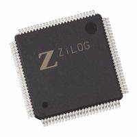
EZ80L92AZ050SG Zilog, EZ80L92AZ050SG Datasheet - Page 46

EZ80L92AZ050SG
Manufacturer Part Number
EZ80L92AZ050SG
Description
IC WEBSERVER 50MHZ 100LQFP
Manufacturer
Zilog
Datasheet
1.EZ80L92AZ020SG.pdf
(231 pages)
Specifications of EZ80L92AZ050SG
Processor Type
eZ80
Features
High Speed, Single-Cycle Instruction-Fetch
Speed
50MHz
Voltage
3.3V
Mounting Type
Surface Mount
Package / Case
100-LQFP
Processor Series
EZ80L92x
Core
eZ80
Data Bus Width
8 bit
Program Memory Size
64 KB
Interface Type
I2C, SPI, UART
Maximum Clock Frequency
50 MHz
Number Of Programmable I/os
24
Number Of Timers
6
Operating Supply Voltage
3 V to 3.6 V
Maximum Operating Temperature
+ 70 C
Mounting Style
SMD/SMT
Development Tools By Supplier
eZ80L920210ZCO
Minimum Operating Temperature
0 C
Lead Free Status / RoHS Status
Lead free / RoHS Compliant
Other names
269-3878
EZ80L92AZ050SG
EZ80L92AZ050SG
Available stocks
Company
Part Number
Manufacturer
Quantity
Price
Company:
Part Number:
EZ80L92AZ050SG
Manufacturer:
Everlight
Quantity:
12 000
- Current page: 46 of 231
- Download datasheet (3Mb)
PS013014-0107
Note:
Writing a 1 to the Port x Data register outputs a High at the pin. Writing a 0 to the Port x
Data register results in a high-impedance output.
GPIO Mode 5.
GPIO Mode 6.
ing edge on the pin cause an interrupt request to be sent to the eZ80
the Port x Data register bit position resets the corresponding interrupt request. Writing 0
produces no effect. You must set the Port x Data register prior to entering the edge-
triggered interrupt mode.
GPIO Mode 7.
alternate (secondary) functions assigned to the pin. For example, the alternate mode
function for PC7 is RI1 and the alternate mode function for PB4 is the Timer 4 Out. When
GPIO Mode 7 is enabled, the pin output data and pin tristated control come from the
alternate function's data output and tristate control, respectively. The value in the Port x
Data register has no effect on operation.
Input signals are sampled by the system clock before being passed to the alternate
function input.
GPIO Mode 8.
request is generated when the level at the pin is the same as the level stored in the Port x
Data register. The port pin value is sampled by the system clock. The input pin must be
held at the selected interrupt level for a minimum of 2 clock periods to initiate an interrupt.
The interrupt request remains active as long as this condition is maintained at the external
source.
GPIO Mode 9.
value in the Port x Data register determines if a positive or negative edge causes an
interrupt request. A 0 in the Port x Data register bit sets the selected pin to generate an
interrupt request for falling edges. A 1 in the Port x Data register bit sets the selected pin to
generate an interrupt request for rising edges. The interrupt request remains active until a 1
is written to the corresponding interrupt request of the Port x Data register bit. Writing a 0
produces no effect on operation. You must set the Port x Data register before entering the
edge-triggered interrupt mode.
A simplified block diagram of a GPIO port pin is illustrated in
Reserved. This pin generates high-impedance output.
This bit enables a dual edge-triggered interrupt mode. Both rising and fall-
For Ports B, C, and D, this port pin is configured to pass control over to the
The port pin is configured for level-sensitive interrupt modes. An interrupt
The port pin is configured for single edge-triggered interrupt mode. The
General-Purpose Input/Output
Figure
Product Specification
®
CPU. Writing 1 to
3.
eZ80L92 MCU
40
Related parts for EZ80L92AZ050SG
Image
Part Number
Description
Manufacturer
Datasheet
Request
R

Part Number:
Description:
Communication Controllers, ZILOG INTELLIGENT PERIPHERAL CONTROLLER (ZIP)
Manufacturer:
Zilog, Inc.
Datasheet:

Part Number:
Description:
KIT DEV FOR Z8 ENCORE 16K TO 64K
Manufacturer:
Zilog
Datasheet:

Part Number:
Description:
KIT DEV Z8 ENCORE XP 28-PIN
Manufacturer:
Zilog
Datasheet:

Part Number:
Description:
DEV KIT FOR Z8 ENCORE 8K/4K
Manufacturer:
Zilog
Datasheet:

Part Number:
Description:
KIT DEV Z8 ENCORE XP 28-PIN
Manufacturer:
Zilog
Datasheet:

Part Number:
Description:
DEV KIT FOR Z8 ENCORE 4K TO 8K
Manufacturer:
Zilog
Datasheet:

Part Number:
Description:
CMOS Z8 microcontroller. ROM 16 Kbytes, RAM 256 bytes, speed 16 MHz, 32 lines I/O, 3.0V to 5.5V
Manufacturer:
Zilog, Inc.
Datasheet:

Part Number:
Description:
Low-cost microcontroller. 512 bytes ROM, 61 bytes RAM, 8 MHz
Manufacturer:
Zilog, Inc.
Datasheet:

Part Number:
Description:
Z8 4K OTP Microcontroller
Manufacturer:
Zilog, Inc.
Datasheet:

Part Number:
Description:
CMOS SUPER8 ROMLESS MCU
Manufacturer:
Zilog, Inc.
Datasheet:

Part Number:
Description:
SL1866 CMOSZ8 OTP Microcontroller
Manufacturer:
Zilog, Inc.
Datasheet:

Part Number:
Description:
SL1866 CMOSZ8 OTP Microcontroller
Manufacturer:
Zilog, Inc.
Datasheet:

Part Number:
Description:
OTP (KB) = 1, RAM = 125, Speed = 12, I/O = 14, 8-bit Timers = 2, Comm Interfaces Other Features = Por, LV Protect, Voltage = 4.5-5.5V
Manufacturer:
Zilog, Inc.
Datasheet:

Part Number:
Description:
Manufacturer:
Zilog, Inc.
Datasheet:


