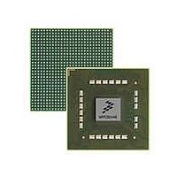
MPC8544VTALF Freescale Semiconductor, MPC8544VTALF Datasheet - Page 1064

MPC8544VTALF
Manufacturer Part Number
MPC8544VTALF
Description
MPU POWERQUICC III 783-PBGA
Manufacturer
Freescale Semiconductor
Datasheets
1.MPC8544VTALF.pdf
(117 pages)
2.MPC8544VTALF.pdf
(2 pages)
3.MPC8544VTALF.pdf
(1340 pages)
Specifications of MPC8544VTALF
Processor Type
MPC85xx PowerQUICC III 32-Bit
Speed
667MHz
Voltage
1V
Mounting Type
Surface Mount
Package / Case
783-FCPBGA
Processor Series
MPC85xx
Core
e500
Data Bus Width
32 bit
Maximum Clock Frequency
667 MHz
Maximum Operating Temperature
+ 105 C
Mounting Style
SMD/SMT
Data Ram Size
32 KB
I/o Voltage
1.8 V, 3.3 V
Interface Type
I2C, HSSI, DUART
Minimum Operating Temperature
0 C
Lead Free Status / RoHS Status
Lead free / RoHS Compliant
Features
-
Lead Free Status / Rohs Status
Lead free / RoHS Compliant
Available stocks
Company
Part Number
Manufacturer
Quantity
Price
Company:
Part Number:
MPC8544VTALF
Manufacturer:
Freescale Semiconductor
Quantity:
10 000
Company:
Part Number:
MPC8544VTALFA
Manufacturer:
Freescale Semiconductor
Quantity:
10 000
- Current page: 1064 of 1340
- Download datasheet (12Mb)
PCI Express Interface Controller
The fields of the PCI Express configuration address register are described in
Both root complex (RC) and endpoint (EP) configuration headers contain 4096 bytes of address space. To
access a register within the header, both the extended register number and the register number fields are
concatenated to form the 4-byte aligned address of the register. That is, the register address is extended
register number || register number || 0b00.
18.3.2.2
The PCI Express configuration data register, show in
configuration access. Note that accesses of 1, 2, or 4 bytes to the PCI Express configuration data register
are allowed. Also note that accesses to the little-endian PCI Express configuration space must be properly
formatted. See
The fields of the PCI Express configuration data register are described in
18-10
16–20
21–23
24–29
30–31
8–15
0–31
Bits
Bits
1–3
4–7
0
Offset 0x004
Reset
Data
Name
EXTREGN
FUNCN
REGN
Name
BUSN
DEVN
W
R
EN
—
—
PCI Express Configuration Data Register (PEX_CONFIG_DATA)
MPC8544E PowerQUICC III Integrated Host Processor Family Reference Manual, Rev. 1
0
Section 18.4.1.2.1, “Byte Order for Configuration
Figure 18-3. PCI Express Configuration Data Register (PEX_CONFIG_DATA)
A read or write to this register starts a PCI Express configuration cycle if the PEX_CONFIG_ADDR enable
bit is set (PEX_CONFIG_ADDR[EN] = 1).
Enable. This bit allows a PCI Express configuration access when PEX_CONFIG_DATA is accessed. If
this bit is cleared, writing to PEX_CONFIG_DATA has no effect and reading PEX_CONFIG_DATA
returns unknown data.
Reserved
is, the registers in the offset range from 0x100 to 0xFFF).
Function number. Function to access within specified device
Reserved
Extended register number. This field allows access to extended PCI Express configuration space (that
Bus number. PCI bus number to access
Device number. Device number to access on specified bus
Register number. 32-bit register to access within specified device
Table 18-4. PEX_CONFIG_ADDR Field Descriptions
Table 18-5. PEX_CONFIG_DATA Field Descriptions
Figure
All zeros
Data
Description
Description
18-3, is a 32-bit port for internal and external
Transactions,” for more information.
Table
Table
18-5.
18-4.
Access: Read/Write
Freescale Semiconductor
31
Related parts for MPC8544VTALF
Image
Part Number
Description
Manufacturer
Datasheet
Request
R
Part Number:
Description:
Manufacturer:
Freescale Semiconductor, Inc
Datasheet:
Part Number:
Description:
Manufacturer:
Freescale Semiconductor, Inc
Datasheet:
Part Number:
Description:
Manufacturer:
Freescale Semiconductor, Inc
Datasheet:
Part Number:
Description:
Manufacturer:
Freescale Semiconductor, Inc
Datasheet:
Part Number:
Description:
Manufacturer:
Freescale Semiconductor, Inc
Datasheet:
Part Number:
Description:
Manufacturer:
Freescale Semiconductor, Inc
Datasheet:
Part Number:
Description:
Manufacturer:
Freescale Semiconductor, Inc
Datasheet:
Part Number:
Description:
Manufacturer:
Freescale Semiconductor, Inc
Datasheet:
Part Number:
Description:
Manufacturer:
Freescale Semiconductor, Inc
Datasheet:
Part Number:
Description:
Manufacturer:
Freescale Semiconductor, Inc
Datasheet:
Part Number:
Description:
Manufacturer:
Freescale Semiconductor, Inc
Datasheet:
Part Number:
Description:
Manufacturer:
Freescale Semiconductor, Inc
Datasheet:
Part Number:
Description:
Manufacturer:
Freescale Semiconductor, Inc
Datasheet:
Part Number:
Description:
Manufacturer:
Freescale Semiconductor, Inc
Datasheet:
Part Number:
Description:
Manufacturer:
Freescale Semiconductor, Inc
Datasheet:


