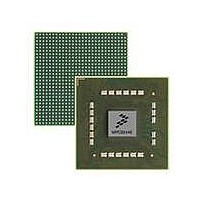
MPC8544VTALF Freescale Semiconductor, MPC8544VTALF Datasheet - Page 346

MPC8544VTALF
Manufacturer Part Number
MPC8544VTALF
Description
MPU POWERQUICC III 783-PBGA
Manufacturer
Freescale Semiconductor
Datasheets
1.MPC8544VTALF.pdf
(117 pages)
2.MPC8544VTALF.pdf
(2 pages)
3.MPC8544VTALF.pdf
(1340 pages)
Specifications of MPC8544VTALF
Processor Type
MPC85xx PowerQUICC III 32-Bit
Speed
667MHz
Voltage
1V
Mounting Type
Surface Mount
Package / Case
783-FCPBGA
Processor Series
MPC85xx
Core
e500
Data Bus Width
32 bit
Maximum Clock Frequency
667 MHz
Maximum Operating Temperature
+ 105 C
Mounting Style
SMD/SMT
Data Ram Size
32 KB
I/o Voltage
1.8 V, 3.3 V
Interface Type
I2C, HSSI, DUART
Minimum Operating Temperature
0 C
Lead Free Status / RoHS Status
Lead free / RoHS Compliant
Features
-
Lead Free Status / Rohs Status
Lead free / RoHS Compliant
Available stocks
Company
Part Number
Manufacturer
Quantity
Price
Company:
Part Number:
MPC8544VTALF
Manufacturer:
Freescale Semiconductor
Quantity:
10 000
Company:
Part Number:
MPC8544VTALFA
Manufacturer:
Freescale Semiconductor
Quantity:
10 000
- Current page: 346 of 1340
- Download datasheet (12Mb)
DDR Memory Controller
9-22
17–23
24–25
Bits
14
15
16
26
27
28
29
BA_INTLV_CTL
x32_EN
PCHB8
2T_EN
NCAP
Name
HSE
—
—
—
MPC8544E PowerQUICC III Integrated Host Processor Family Reference Manual, Rev. 1
Table 9-12. DDR_SDRAM_CFG Field Descriptions (continued)
precharge. If one of these devices is used, then this bit will need to be set if auto precharge is used.
0 DRAMs in system support concurrent auto-precharge.
1 DRAMs in system do not support concurrent auto-precharge.
Reserved
Enable 2T timing.
0 1T timing is enabled. The DRAM command/address are held for only 1 cycle on the DRAM bus.
1 2T timing is enabled. The DRAM command/address are held for 2 full cycles on the DRAM bus
Note that RD_EN and 2T_EN must not both be set at the same time.
(‘ x ’ denotes a don’t care bit value. All unlisted field values are reserved.)
0000000 No external memory banks are interleaved
1000000 External memory banks 0 and 1 are interleaved
0100000 External memory banks 2 and 3 are interleaved
1100000 External memory banks 0 and 1 are interleaved together and
xx 00100 External memory banks 0 through 3 are all interleaved together
Reserved
0 Either x8 or x16 discrete DRAM chips are used. In this mode, each data byte has a dedicated
1 x32 discrete DRAM chips are used. In this mode, DQS0 will be used to capture DQ[0:31], DQS4
0 MA[10] will be used to indicate the auto-precharge and precharge all commands.
1 MA[8] will be used to indicate the auto-precharge and precharge all commands.
If x32_EN is cleared, then PCHB8 should be cleared as well.
Sets I/O driver impedance to half strength. This impedance will be used by the MDIC,
address/command, data, and clock impedance values, but only if automatic hardware calibration is
disabled and the corresponding group's software override is disabled in the DDR control driver
register(s) described in
0 I/O driver impedance will be configured to full strength.
1 I/O driver impedance will be configured to half strength.
Reserved
Non-concurrent auto-precharge. Some older DDR DRAMs do not support concurrent auto
Bank (chip select) interleaving control. Set this field only if you wish to use bank interleaving.
x32 enable.
Precharge bit 8 enable.
Global half-strength override
for every DRAM transaction. However, the chip select is only held for the second cycle.
corresponding data strobe.
will be used to capture DQ[32:63] and DQS8 will be used to capture ECC[0:7].
banks 2 and 3 are interleaved together
Section 19.4.1.21, “DDR Control Driver Register (DDRCDR).”
Description
S
Freescale Semiconductor
Related parts for MPC8544VTALF
Image
Part Number
Description
Manufacturer
Datasheet
Request
R
Part Number:
Description:
Manufacturer:
Freescale Semiconductor, Inc
Datasheet:
Part Number:
Description:
Manufacturer:
Freescale Semiconductor, Inc
Datasheet:
Part Number:
Description:
Manufacturer:
Freescale Semiconductor, Inc
Datasheet:
Part Number:
Description:
Manufacturer:
Freescale Semiconductor, Inc
Datasheet:
Part Number:
Description:
Manufacturer:
Freescale Semiconductor, Inc
Datasheet:
Part Number:
Description:
Manufacturer:
Freescale Semiconductor, Inc
Datasheet:
Part Number:
Description:
Manufacturer:
Freescale Semiconductor, Inc
Datasheet:
Part Number:
Description:
Manufacturer:
Freescale Semiconductor, Inc
Datasheet:
Part Number:
Description:
Manufacturer:
Freescale Semiconductor, Inc
Datasheet:
Part Number:
Description:
Manufacturer:
Freescale Semiconductor, Inc
Datasheet:
Part Number:
Description:
Manufacturer:
Freescale Semiconductor, Inc
Datasheet:
Part Number:
Description:
Manufacturer:
Freescale Semiconductor, Inc
Datasheet:
Part Number:
Description:
Manufacturer:
Freescale Semiconductor, Inc
Datasheet:
Part Number:
Description:
Manufacturer:
Freescale Semiconductor, Inc
Datasheet:
Part Number:
Description:
Manufacturer:
Freescale Semiconductor, Inc
Datasheet:


