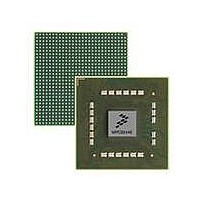
MPC8544VTALF Freescale Semiconductor, MPC8544VTALF Datasheet - Page 155

MPC8544VTALF
Manufacturer Part Number
MPC8544VTALF
Description
MPU POWERQUICC III 783-PBGA
Manufacturer
Freescale Semiconductor
Datasheets
1.MPC8544VTALF.pdf
(117 pages)
2.MPC8544VTALF.pdf
(2 pages)
3.MPC8544VTALF.pdf
(1340 pages)
Specifications of MPC8544VTALF
Processor Type
MPC85xx PowerQUICC III 32-Bit
Speed
667MHz
Voltage
1V
Mounting Type
Surface Mount
Package / Case
783-FCPBGA
Processor Series
MPC85xx
Core
e500
Data Bus Width
32 bit
Maximum Clock Frequency
667 MHz
Maximum Operating Temperature
+ 105 C
Mounting Style
SMD/SMT
Data Ram Size
32 KB
I/o Voltage
1.8 V, 3.3 V
Interface Type
I2C, HSSI, DUART
Minimum Operating Temperature
0 C
Lead Free Status / RoHS Status
Lead free / RoHS Compliant
Features
-
Lead Free Status / Rohs Status
Lead free / RoHS Compliant
Available stocks
Company
Part Number
Manufacturer
Quantity
Price
Company:
Part Number:
MPC8544VTALF
Manufacturer:
Freescale Semiconductor
Quantity:
10 000
Company:
Part Number:
MPC8544VTALFA
Manufacturer:
Freescale Semiconductor
Quantity:
10 000
- Current page: 155 of 1340
- Download datasheet (12Mb)
TSEC3_GTX_CLK TSEC3 transmit clock out
3.2
The signals that serve alternate functions as configuration input signals during system reset are
summarized in
Chapter 4, “Reset, Clocking, and Initialization.”
Note that throughout this document, the reset configuration signals are described as being sampled at the
negation of HRESET. However, there is a setup and hold time for these signals relative to the rising edge
of HRESET, as described in the MPC8544E Integrated Processor Hardware Specifications. Note that the
PLL configuration signals have different setup and hold time requirements than the other reset
configuration signals.
The reset configuration signals are multiplexed with other functional signals. The values on these signals
during reset are interpreted to be logic one or zero, regardless of whether the functional signal name is
defined as active-low. Most of the reset configuration signals have internal pull-up resistors so that if the
signals are not driven, the default value is high (a one), as shown in the table. Some signals do not have
Freescale Semiconductor
UART_SOUT[0:1]
TSEC3_RXD[7:0]
TSEC3_TXD[1:0]
TSEC3_TXD[6:4]
TSEC3_RX_CLK
TSEC3_TX_CLK
TSEC3_RX_ER
UART_CTS[0:1]
UART_RTS[0:1]
TSEC3_RX_DV
TSEC3_TX_EN
TSEC3_TX_ER
UART_SIN[0:1]
TSEC3_TXD2
TSEC3_TXD3
TSEC3_TXD7
Name
UDE
Configuration Signals Sampled at Reset
MPC8544E PowerQUICC III Integrated Host Processor Family Reference Manual, Rev. 1
Table
TSEC3 receive clock
TSEC3 receive data valid
TSEC3 receive error
TSEC3 receive data 7–0
TSEC3 transmit clock in
TSEC3 transmit enable
TSEC3 transmit error
TSEC3 transmit data 1–0
TSEC3 transmit data [6:4]
TSEC3 transmit data 2
TSEC3 transmit data 3
TSEC3 transmit data 7
DUART clear to send
DUART ready to send
DUART serial data in
DUART serial data out
Unconditional debug event
Table 3-2. MPC8544E Alphabetical Signal Reference (continued)
3-3. The detailed interpretation of their voltage levels during reset is described in
Description
Functional
Dual UART
Dual UART
Dual UART
Dual UART
eTSEC3
eTSEC3
eTSEC3
eTSEC3
eTSEC3
eTSEC3
eTSEC3
eTSEC3
eTSEC3
eTSEC3
eTSEC3
eTSEC3
eTSEC3
Block
PIC
Alternate Function(s)
cfg_etsec3_prtcl[1:0]
cfg_etsec3_reduce
/cfg_io_ports[0:2]
cfg_etsec3_serial
FIFO3_RXD[7:0]
FIFO3_TXD[1:0]
FIFO3_TXD[6:4]
FIFO3_RX_CLK
FIFO3_TX_CLK
FIFO3_RX_DV
FIFO3_RX_ER
FIFO3_TX_EN
FIFO3_TX_ER
FIFO3_TXD2
FIFO3_TXD3
FIFO3_TXD7
—
—
—
—
—
—
Signals
No. of
1
1
1
1
8
1
1
1
2
3
1
1
1
2
2
2
2
1
I/O
O
O
O
O
O
O
O
O
O
O
I
I
I
I
I
I
I
I
Signal Descriptions
15-2/15-9
15-2/15-9
15-2/15-9
15-2/15-9
15-2/15-9
15-2/15-9
15-2/15-9
15-2/15-9
15-2/15-9
15-2/15-9
15-2/15-9
15-2/15-9
15-2/15-9
13-2/13-3
13-2/13-3
13-2/13-3
13-2/13-3
10-5/10-8
Table/
Page
3-15
Related parts for MPC8544VTALF
Image
Part Number
Description
Manufacturer
Datasheet
Request
R
Part Number:
Description:
Manufacturer:
Freescale Semiconductor, Inc
Datasheet:
Part Number:
Description:
Manufacturer:
Freescale Semiconductor, Inc
Datasheet:
Part Number:
Description:
Manufacturer:
Freescale Semiconductor, Inc
Datasheet:
Part Number:
Description:
Manufacturer:
Freescale Semiconductor, Inc
Datasheet:
Part Number:
Description:
Manufacturer:
Freescale Semiconductor, Inc
Datasheet:
Part Number:
Description:
Manufacturer:
Freescale Semiconductor, Inc
Datasheet:
Part Number:
Description:
Manufacturer:
Freescale Semiconductor, Inc
Datasheet:
Part Number:
Description:
Manufacturer:
Freescale Semiconductor, Inc
Datasheet:
Part Number:
Description:
Manufacturer:
Freescale Semiconductor, Inc
Datasheet:
Part Number:
Description:
Manufacturer:
Freescale Semiconductor, Inc
Datasheet:
Part Number:
Description:
Manufacturer:
Freescale Semiconductor, Inc
Datasheet:
Part Number:
Description:
Manufacturer:
Freescale Semiconductor, Inc
Datasheet:
Part Number:
Description:
Manufacturer:
Freescale Semiconductor, Inc
Datasheet:
Part Number:
Description:
Manufacturer:
Freescale Semiconductor, Inc
Datasheet:
Part Number:
Description:
Manufacturer:
Freescale Semiconductor, Inc
Datasheet:


