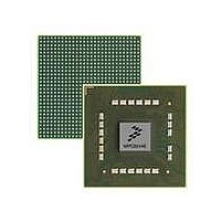
MPC8544VTALF Freescale Semiconductor, MPC8544VTALF Datasheet - Page 215

MPC8544VTALF
Manufacturer Part Number
MPC8544VTALF
Description
MPU POWERQUICC III 783-PBGA
Manufacturer
Freescale Semiconductor
Datasheets
1.MPC8544VTALF.pdf
(117 pages)
2.MPC8544VTALF.pdf
(2 pages)
3.MPC8544VTALF.pdf
(1340 pages)
Specifications of MPC8544VTALF
Processor Type
MPC85xx PowerQUICC III 32-Bit
Speed
667MHz
Voltage
1V
Mounting Type
Surface Mount
Package / Case
783-FCPBGA
Processor Series
MPC85xx
Core
e500
Data Bus Width
32 bit
Maximum Clock Frequency
667 MHz
Maximum Operating Temperature
+ 105 C
Mounting Style
SMD/SMT
Data Ram Size
32 KB
I/o Voltage
1.8 V, 3.3 V
Interface Type
I2C, HSSI, DUART
Minimum Operating Temperature
0 C
Lead Free Status / RoHS Status
Lead free / RoHS Compliant
Features
-
Lead Free Status / Rohs Status
Lead free / RoHS Compliant
Available stocks
Company
Part Number
Manufacturer
Quantity
Price
Company:
Part Number:
MPC8544VTALF
Manufacturer:
Freescale Semiconductor
Quantity:
10 000
Company:
Part Number:
MPC8544VTALFA
Manufacturer:
Freescale Semiconductor
Quantity:
10 000
- Current page: 215 of 1340
- Download datasheet (12Mb)
5.13
This section provides an overview of the architectural differences and compatibilities of the e500 core
compared with the AIM Power Architecture technology. The two levels of the e500 programming
environment are as follows:
Like all devices that implement the Power Architecture technology, in general, the e500 core supports the
user-level architecture. The following sections are intended to highlight the main differences. For specific
implementation details refer to the relevant chapter.
5.13.1
The following sections generally describe the user and supervisor instruction sets.
5.13.1.1
The e500 core executes legacy user-mode binaries and object files except for the following:
5.13.1.2
The supervisor mode instruction set defined by the PowerPC architecture is compatible with the e500 with
the following exceptions:
Freescale Semiconductor
•
•
•
•
•
•
or disabled from this register. The contents of these registers are reflected to
UPMLCa0–UPMLCa3, which can be read from user mode with mfpmr.
PMLCb0–PMLCb3 provide count scaling for each counter register using configurable threshold
and multiplier values. The threshold is a 6-bit value and the multiplier is a 3-bit encoded value,
allowing eight multiplier values in the range of 1 to 128. Any counter may be configured to
increment only when an event occurs more than [threshold × multiplier] times. The contents of
these registers are reflected to UPMLCb0–UPMLCb3, which can be read from user mode with
mfpmr.
User level—This defines the base user-level instruction set, user-level registers, data types,
memory conventions, and the memory and programming models seen by application
programmers.
Supervisor level—This defines supervisor-level resources typically required by an operating
system, the memory management model, supervisor level registers, and the exception model.
The e500 supports vector and scalar single-precision floating-point operations as part of the SPE.
The e500v2 supports scalar double-precision floating-point instructions. These instructions have
different encoding than the AIM definition of the architecture. Additionally, the e500 core uses
GPRs for floating-point operations, rather than the FPRs defined by the UISA. Most porting of
floating-point operations can be handled by recompiling.
String instructions are not implemented on the e500; therefore, trap emulation must be provided to
ensure backward compatibility.
The MMU architecture is different, so some TLB manipulation instructions have different
semantics.
Legacy Support of Power Architecture Technology
Instruction Set Compatibility
MPC8544E PowerQUICC III Integrated Host Processor Family Reference Manual, Rev. 1
User Instruction Set
Supervisor Instruction Set
Core Complex Overview
5-29
Related parts for MPC8544VTALF
Image
Part Number
Description
Manufacturer
Datasheet
Request
R
Part Number:
Description:
Manufacturer:
Freescale Semiconductor, Inc
Datasheet:
Part Number:
Description:
Manufacturer:
Freescale Semiconductor, Inc
Datasheet:
Part Number:
Description:
Manufacturer:
Freescale Semiconductor, Inc
Datasheet:
Part Number:
Description:
Manufacturer:
Freescale Semiconductor, Inc
Datasheet:
Part Number:
Description:
Manufacturer:
Freescale Semiconductor, Inc
Datasheet:
Part Number:
Description:
Manufacturer:
Freescale Semiconductor, Inc
Datasheet:
Part Number:
Description:
Manufacturer:
Freescale Semiconductor, Inc
Datasheet:
Part Number:
Description:
Manufacturer:
Freescale Semiconductor, Inc
Datasheet:
Part Number:
Description:
Manufacturer:
Freescale Semiconductor, Inc
Datasheet:
Part Number:
Description:
Manufacturer:
Freescale Semiconductor, Inc
Datasheet:
Part Number:
Description:
Manufacturer:
Freescale Semiconductor, Inc
Datasheet:
Part Number:
Description:
Manufacturer:
Freescale Semiconductor, Inc
Datasheet:
Part Number:
Description:
Manufacturer:
Freescale Semiconductor, Inc
Datasheet:
Part Number:
Description:
Manufacturer:
Freescale Semiconductor, Inc
Datasheet:
Part Number:
Description:
Manufacturer:
Freescale Semiconductor, Inc
Datasheet:


