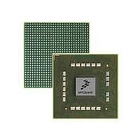
MPC8544VTALF Freescale Semiconductor, MPC8544VTALF Datasheet - Page 654

MPC8544VTALF
Manufacturer Part Number
MPC8544VTALF
Description
MPU POWERQUICC III 783-PBGA
Manufacturer
Freescale Semiconductor
Datasheets
1.MPC8544VTALF.pdf
(117 pages)
2.MPC8544VTALF.pdf
(2 pages)
3.MPC8544VTALF.pdf
(1340 pages)
Specifications of MPC8544VTALF
Processor Type
MPC85xx PowerQUICC III 32-Bit
Speed
667MHz
Voltage
1V
Mounting Type
Surface Mount
Package / Case
783-FCPBGA
Processor Series
MPC85xx
Core
e500
Data Bus Width
32 bit
Maximum Clock Frequency
667 MHz
Maximum Operating Temperature
+ 105 C
Mounting Style
SMD/SMT
Data Ram Size
32 KB
I/o Voltage
1.8 V, 3.3 V
Interface Type
I2C, HSSI, DUART
Minimum Operating Temperature
0 C
Lead Free Status / RoHS Status
Lead free / RoHS Compliant
Features
-
Lead Free Status / Rohs Status
Lead free / RoHS Compliant
Available stocks
Company
Part Number
Manufacturer
Quantity
Price
Company:
Part Number:
MPC8544VTALF
Manufacturer:
Freescale Semiconductor
Quantity:
10 000
Company:
Part Number:
MPC8544VTALFA
Manufacturer:
Freescale Semiconductor
Quantity:
10 000
- Current page: 654 of 1340
- Download datasheet (12Mb)
Local Bus Controller
address during LALE phases. UPM may require LA[27:31] if the LBC is generating its own burst address
sequence.
To illustrate how a large transaction is handled by the LBC,
performing a 32-byte write starting at address 0x5420. Note that during each of the 32 assertions of LALE,
LA[27:31] exactly mirror LAD[27:31], but during data phases, only LAD[0:7] and LDP[0] are driven with
valid data and parity, respectively.
14.4.1.3
The three memory controllers in the LBC generate an internal transfer acknowledge signal, TA, to allow
data on LAD[0:31] to be either sampled (for reads) or changed (on writes). The data sampling/data change
always occurs at the end of the bus cycle in which the LBC asserts TA internally. In LBC debug mode, TA
is also visible externally on the MDVAL signal. GPCM and SDRAM controllers automatically generate
TA according to the timing parameters programmed for them in option and mode registers; a UPM
generates TA only when a UPM pattern has the UTA RAM word bit set.
14-34
LAD[8:31]
LA[27:31]
Note: All address and signal values are shown in hexadecimal.
LAD[0:7]
LDP[1:3]
LDP[0]
LCLK
LCS n
LALE
LWE
D(Bk) = k
MPC8544E PowerQUICC III Integrated Host Processor Family Reference Manual, Rev. 1
Data Transfer Acknowledge (TA)
Figure 14-21. Example of 8-Bit GPCM Writing 32 Bytes to Address 0x5420
th
00
54
0
20
0
of 32 data bytes, P(Bk) = parity bit of k
00
D(B0)
P(B0)
00
54
21
0
0
01
D(B1)
P(B1)
00
54
22
0
0
02
D(B2)
P(B2)
th
03
00
54
23
0
0
data byte.
Figure 14-21
1C
54
3D
00
0
0
1D
D(B29)
P(B29)
shows LBC signals for GPCM
54
3E
00
0
0
1E
D(B30)
P(B30)
Freescale Semiconductor
00
54
3F
0
0
1F
D(B31)
P(B31)
Related parts for MPC8544VTALF
Image
Part Number
Description
Manufacturer
Datasheet
Request
R
Part Number:
Description:
Manufacturer:
Freescale Semiconductor, Inc
Datasheet:
Part Number:
Description:
Manufacturer:
Freescale Semiconductor, Inc
Datasheet:
Part Number:
Description:
Manufacturer:
Freescale Semiconductor, Inc
Datasheet:
Part Number:
Description:
Manufacturer:
Freescale Semiconductor, Inc
Datasheet:
Part Number:
Description:
Manufacturer:
Freescale Semiconductor, Inc
Datasheet:
Part Number:
Description:
Manufacturer:
Freescale Semiconductor, Inc
Datasheet:
Part Number:
Description:
Manufacturer:
Freescale Semiconductor, Inc
Datasheet:
Part Number:
Description:
Manufacturer:
Freescale Semiconductor, Inc
Datasheet:
Part Number:
Description:
Manufacturer:
Freescale Semiconductor, Inc
Datasheet:
Part Number:
Description:
Manufacturer:
Freescale Semiconductor, Inc
Datasheet:
Part Number:
Description:
Manufacturer:
Freescale Semiconductor, Inc
Datasheet:
Part Number:
Description:
Manufacturer:
Freescale Semiconductor, Inc
Datasheet:
Part Number:
Description:
Manufacturer:
Freescale Semiconductor, Inc
Datasheet:
Part Number:
Description:
Manufacturer:
Freescale Semiconductor, Inc
Datasheet:
Part Number:
Description:
Manufacturer:
Freescale Semiconductor, Inc
Datasheet:


