C8051F930-TB Silicon Laboratories Inc, C8051F930-TB Datasheet - Page 14
C8051F930-TB
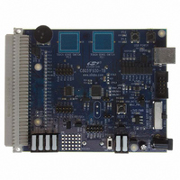
Manufacturer Part Number
C8051F930-TB
Description
BOARD TARGET/PROTO W/C8051F930
Manufacturer
Silicon Laboratories Inc
Type
MCUr
Specifications of C8051F930-TB
Contents
Board
Processor To Be Evaluated
C8051F930
Processor Series
C8051F9xx
Data Bus Width
8 bit
Interface Type
I2C, UART, SPI
Maximum Operating Temperature
+ 85 C
Minimum Operating Temperature
- 40 C
Operating Supply Voltage
0.9 V to 3.6 V
Lead Free Status / RoHS Status
Lead free / RoHS Compliant
For Use With/related Products
C8051F930
Lead Free Status / Rohs Status
Lead free / RoHS Compliant
Other names
336-1472


C8051F93x-C8051F92x
13. Flash Memory
14. Power Management
15. Cyclic Redundancy Check Unit (CRC0)
16. On-Chip DC-DC Converter (DC0)
17. Voltage Regulator (VREG0)
18. Reset Sources
19. Clocking Sources
20. SmaRTClock (Real Time Clock)
21. Port Input/Output
22. SMBus
23. UART0
24. Enhanced Serial Peripheral Interface (SPI0 and SPI1)
25. Timers
26. Programmable Counter Array
27. C2 Interface
14
Table 13.1. Flash Security Summary . . . . . . . . . . . . . . . . . . . . . . . . . . . . . . . . . . 148
Table 14.1. Power Modes . . . . . . . . . . . . . . . . . . . . . . . . . . . . . . . . . . . . . . . . . . . 156
Table 15.1. Example 16-bit CRC Outputs . . . . . . . . . . . . . . . . . . . . . . . . . . . . . . . 165
Table 16.1. IPeak Inductor Current Limit Settings . . . . . . . . . . . . . . . . . . . . . . . . . 172
Table 19.1. Recommended XFCN Settings for Crystal Mode . . . . . . . . . . . . . . . . 189
Table 19.2. Recommended XFCN Settings for RC and C modes . . . . . . . . . . . . . 190
Table 20.1. SmaRTClock Internal Registers ......................................................... 197
Table 20.2. SmaRTClock Load Capacitance Settings . . . . . . . . . . . . . . . . . . . . . 203
Table 20.3. SmaRTClock Bias Settings . . . . . . . . . . . . . . . . . . . . . . . . . . . . . . . . 205
Table 21.1. Port I/O Assignment for Analog Functions . . . . . . . . . . . . . . . . . . . . . 214
Table 21.2. Port I/O Assignment for Digital Functions . . . . . . . . . . . . . . . . . . . . . . 215
Table 21.3. Port I/O Assignment for External Digital Event Capture Functions . . 215
Table 22.1. SMBus Clock Source Selection . . . . . . . . . . . . . . . . . . . . . . . . . . . . . 238
Table 22.2. Minimum SDA Setup and Hold Times . . . . . . . . . . . . . . . . . . . . . . . . 239
Table 22.3. Sources for Hardware Changes to SMB0CN . . . . . . . . . . . . . . . . . . . 243
Table 22.4. Hardware Address Recognition Examples (EHACK = 1) . . . . . . . . . . 244
Table 22.5. SMBus Status Decoding With Hardware ACK Generation Disabled
Table 22.6. SMBus Status Decoding With Hardware ACK Generation Enabled
Table 23.1. Timer Settings for Standard Baud Rates
Table 23.2. Timer Settings for Standard Baud Rates
Table 24.1. SPI Slave Timing Parameters . . . . . . . . . . . . . . . . . . . . . . . . . . . . . . 277
Table 25.1. Timer 0 Running Modes . . . . . . . . . . . . . . . . . . . . . . . . . . . . . . . . . . . 280
Table 26.1. PCA Timebase Input Options . . . . . . . . . . . . . . . . . . . . . . . . . . . . . . . 301
Table 26.2. PCA0CPM and PCA0PWM Bit Settings for PCA
Table 26.3. Watchdog Timer Timeout Intervals1 . . . . . . . . . . . . . . . . . . . . . . . . . . 312
(EHACK = 0) . . . . . . . . . . . . . . . . . . . . . . . . . . . . . . . . . . . . . . . . . . . . 251
(EHACK = 1) . . . . . . . . . . . . . . . . . . . . . . . . . . . . . . . . . . . . . . . . . . . . 253
Using The Internal 24.5 MHz Oscillator . . . . . . . . . . . . . . . . . . . . . . . 262
Using an External 22.1184 MHz Oscillator . . . . . . . . . . . . . . . . . . . . . 262
Capture/Compare Modules . . . . . . . . . . . . . . . . . . . . . . . . . . . . . . . . 303
Rev. 1.1
Related parts for C8051F930-TB
Image
Part Number
Description
Manufacturer
Datasheet
Request
R

Part Number:
Description:
SMD/C°/SINGLE-ENDED OUTPUT SILICON OSCILLATOR
Manufacturer:
Silicon Laboratories Inc
Part Number:
Description:
Manufacturer:
Silicon Laboratories Inc
Datasheet:
Part Number:
Description:
N/A N/A/SI4010 AES KEYFOB DEMO WITH LCD RX
Manufacturer:
Silicon Laboratories Inc
Datasheet:
Part Number:
Description:
N/A N/A/SI4010 SIMPLIFIED KEY FOB DEMO WITH LED RX
Manufacturer:
Silicon Laboratories Inc
Datasheet:
Part Number:
Description:
N/A/-40 TO 85 OC/EZLINK MODULE; F930/4432 HIGH BAND (REV E/B1)
Manufacturer:
Silicon Laboratories Inc
Part Number:
Description:
EZLink Module; F930/4432 Low Band (rev e/B1)
Manufacturer:
Silicon Laboratories Inc
Part Number:
Description:
I°/4460 10 DBM RADIO TEST CARD 434 MHZ
Manufacturer:
Silicon Laboratories Inc
Part Number:
Description:
I°/4461 14 DBM RADIO TEST CARD 868 MHZ
Manufacturer:
Silicon Laboratories Inc
Part Number:
Description:
I°/4463 20 DBM RFSWITCH RADIO TEST CARD 460 MHZ
Manufacturer:
Silicon Laboratories Inc
Part Number:
Description:
I°/4463 20 DBM RADIO TEST CARD 868 MHZ
Manufacturer:
Silicon Laboratories Inc
Part Number:
Description:
I°/4463 27 DBM RADIO TEST CARD 868 MHZ
Manufacturer:
Silicon Laboratories Inc
Part Number:
Description:
I°/4463 SKYWORKS 30 DBM RADIO TEST CARD 915 MHZ
Manufacturer:
Silicon Laboratories Inc
Part Number:
Description:
N/A N/A/-40 TO 85 OC/4463 RFMD 30 DBM RADIO TEST CARD 915 MHZ
Manufacturer:
Silicon Laboratories Inc
Part Number:
Description:
I°/4463 20 DBM RADIO TEST CARD 169 MHZ
Manufacturer:
Silicon Laboratories Inc