C8051F930-TB Silicon Laboratories Inc, C8051F930-TB Datasheet - Page 7
C8051F930-TB
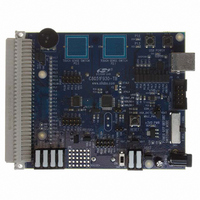
Manufacturer Part Number
C8051F930-TB
Description
BOARD TARGET/PROTO W/C8051F930
Manufacturer
Silicon Laboratories Inc
Type
MCUr
Specifications of C8051F930-TB
Contents
Board
Processor To Be Evaluated
C8051F930
Processor Series
C8051F9xx
Data Bus Width
8 bit
Interface Type
I2C, UART, SPI
Maximum Operating Temperature
+ 85 C
Minimum Operating Temperature
- 40 C
Operating Supply Voltage
0.9 V to 3.6 V
Lead Free Status / RoHS Status
Lead free / RoHS Compliant
For Use With/related Products
C8051F930
Lead Free Status / Rohs Status
Lead free / RoHS Compliant
Other names
336-1472


22. SMBus ................................................................................................................... 233
23. UART0.................................................................................................................... 255
24. Enhanced Serial Peripheral Interface (SPI0 and SPI1)...................................... 263
25. Timers.................................................................................................................... 278
22.1.Supporting Documents ................................................................................... 234
22.2.SMBus Configuration...................................................................................... 234
22.3.SMBus Operation ........................................................................................... 235
22.4.Using the SMBus............................................................................................ 237
22.5.SMBus Transfer Modes.................................................................................. 247
22.6.SMBus Status Decoding................................................................................. 250
23.1.Enhanced Baud Rate Generation................................................................... 256
23.2.Operational Modes ......................................................................................... 257
23.3.Multiprocessor Communications .................................................................... 258
24.1.Signal Descriptions......................................................................................... 264
24.2.SPI Master Mode Operation ........................................................................... 265
24.3.SPI Slave Mode Operation ............................................................................. 267
24.4.SPI Interrupt Sources ..................................................................................... 267
24.5.Serial Clock Phase and Polarity ..................................................................... 268
24.6.SPI Special Function Registers ...................................................................... 270
25.1.Timer 0 and Timer 1 ....................................................................................... 280
25.2.Timer 2 .......................................................................................................... 288
22.3.1.Transmitter Vs. Receiver........................................................................ 235
22.3.2.Arbitration............................................................................................... 235
22.3.3.Clock Low Extension.............................................................................. 236
22.3.4.SCL Low Timeout................................................................................... 236
22.3.5.SCL High (SMBus Free) Timeout .......................................................... 236
22.4.1.SMBus Configuration Register............................................................... 238
22.4.2.SMB0CN Control Register ..................................................................... 241
22.4.3.Hardware Slave Address Recognition ................................................... 244
22.4.4.Data Register ......................................................................................... 246
22.5.1.Write Sequence (Master) ....................................................................... 247
22.5.2.Read Sequence (Master) ....................................................................... 248
22.5.3.Write Sequence (Slave) ......................................................................... 249
22.5.4.Read Sequence (Slave) ......................................................................... 250
23.2.1.8-Bit UART ............................................................................................. 257
23.2.2.9-Bit UART ............................................................................................. 258
24.1.1.Master Out, Slave In (MOSI).................................................................. 264
24.1.2.Master In, Slave Out (MISO).................................................................. 264
24.1.3.Serial Clock (SCK) ................................................................................. 264
24.1.4.Slave Select (NSS) ................................................................................ 264
25.1.1.Mode 0: 13-bit Counter/Timer ................................................................ 280
25.1.2.Mode 1: 16-bit Counter/Timer ................................................................ 281
25.1.3.Mode 2: 8-bit Counter/Timer with Auto-Reload...................................... 282
25.1.4.Mode 3: Two 8-bit Counter/Timers (Timer 0 Only)................................. 283
25.2.1.16-bit Timer with Auto-Reload................................................................ 288
Rev. 1.1
C8051F93x-C8051F92x
7
Related parts for C8051F930-TB
Image
Part Number
Description
Manufacturer
Datasheet
Request
R

Part Number:
Description:
SMD/C°/SINGLE-ENDED OUTPUT SILICON OSCILLATOR
Manufacturer:
Silicon Laboratories Inc
Part Number:
Description:
Manufacturer:
Silicon Laboratories Inc
Datasheet:
Part Number:
Description:
N/A N/A/SI4010 AES KEYFOB DEMO WITH LCD RX
Manufacturer:
Silicon Laboratories Inc
Datasheet:
Part Number:
Description:
N/A N/A/SI4010 SIMPLIFIED KEY FOB DEMO WITH LED RX
Manufacturer:
Silicon Laboratories Inc
Datasheet:
Part Number:
Description:
N/A/-40 TO 85 OC/EZLINK MODULE; F930/4432 HIGH BAND (REV E/B1)
Manufacturer:
Silicon Laboratories Inc
Part Number:
Description:
EZLink Module; F930/4432 Low Band (rev e/B1)
Manufacturer:
Silicon Laboratories Inc
Part Number:
Description:
I°/4460 10 DBM RADIO TEST CARD 434 MHZ
Manufacturer:
Silicon Laboratories Inc
Part Number:
Description:
I°/4461 14 DBM RADIO TEST CARD 868 MHZ
Manufacturer:
Silicon Laboratories Inc
Part Number:
Description:
I°/4463 20 DBM RFSWITCH RADIO TEST CARD 460 MHZ
Manufacturer:
Silicon Laboratories Inc
Part Number:
Description:
I°/4463 20 DBM RADIO TEST CARD 868 MHZ
Manufacturer:
Silicon Laboratories Inc
Part Number:
Description:
I°/4463 27 DBM RADIO TEST CARD 868 MHZ
Manufacturer:
Silicon Laboratories Inc
Part Number:
Description:
I°/4463 SKYWORKS 30 DBM RADIO TEST CARD 915 MHZ
Manufacturer:
Silicon Laboratories Inc
Part Number:
Description:
N/A N/A/-40 TO 85 OC/4463 RFMD 30 DBM RADIO TEST CARD 915 MHZ
Manufacturer:
Silicon Laboratories Inc
Part Number:
Description:
I°/4463 20 DBM RADIO TEST CARD 169 MHZ
Manufacturer:
Silicon Laboratories Inc