C8051F930-TB Silicon Laboratories Inc, C8051F930-TB Datasheet - Page 185
C8051F930-TB
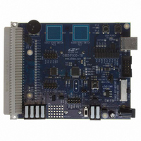
Manufacturer Part Number
C8051F930-TB
Description
BOARD TARGET/PROTO W/C8051F930
Manufacturer
Silicon Laboratories Inc
Type
MCUr
Specifications of C8051F930-TB
Contents
Board
Processor To Be Evaluated
C8051F930
Processor Series
C8051F9xx
Data Bus Width
8 bit
Interface Type
I2C, UART, SPI
Maximum Operating Temperature
+ 85 C
Minimum Operating Temperature
- 40 C
Operating Supply Voltage
0.9 V to 3.6 V
Lead Free Status / RoHS Status
Lead free / RoHS Compliant
For Use With/related Products
C8051F930
Lead Free Status / Rohs Status
Lead free / RoHS Compliant
Other names
336-1472


18.7. Flash Error Reset
If a Flash read/write/erase or program read targets an illegal address, a system reset is generated. This
may occur due to any of the following:
•
•
•
•
•
The FERROR bit (RSTSRC.6) is set following a Flash error reset. The state of the RST pin is unaffected by
this reset.
18.8. SmaRTClock (Real Time Clock) Reset
The SmaRTClock can generate a system reset on two events: SmaRTClock Oscillator Fail or SmaRT-
Clock Alarm. The SmaRTClock Oscillator Fail event occurs when the SmaRTClock Missing Clock Detector
is enabled and the SmaRTClock clock is below approximately 20 kHz. A SmaRTClock alarm event occurs
when the SmaRTClock Alarm is enabled and the SmaRTClock timer value matches the ALARMn regis-
ters. The SmaRTClock can be configured as a reset source by writing a 1 to the RTC0RE flag (RST-
SRC.7). The SmaRTClock reset remains functional even when the device is in the low power Suspend or
Sleep mode. The state of the RST pin is unaffected by this reset.
18.9. Software Reset
Software may force a reset by writing a 1 to the SWRSF bit (RSTSRC.4). The SWRSF bit will read 1 fol-
lowing a software forced reset. The state of the RST pin is unaffected by this reset.
A Flash write or erase is attempted above user code space. This occurs when PSWE is set to 1 and a
MOVX write operation targets an address above the Lock Byte address.
A Flash read is attempted above user code space. This occurs when a MOVC operation targets an
address above the Lock Byte address.
A Program read is attempted above user code space. This occurs when user code attempts to branch
to an address above the Lock Byte address.
A Flash read, write or erase attempt is restricted due to a Flash security setting (see Section
“13.3. Security Options” on page 147).
A Flash write or erase is attempted while the V
Rev. 1.1
DD
Monitor is disabled.
C8051F93x-C8051F92x
185
Related parts for C8051F930-TB
Image
Part Number
Description
Manufacturer
Datasheet
Request
R

Part Number:
Description:
SMD/C°/SINGLE-ENDED OUTPUT SILICON OSCILLATOR
Manufacturer:
Silicon Laboratories Inc
Part Number:
Description:
Manufacturer:
Silicon Laboratories Inc
Datasheet:
Part Number:
Description:
N/A N/A/SI4010 AES KEYFOB DEMO WITH LCD RX
Manufacturer:
Silicon Laboratories Inc
Datasheet:
Part Number:
Description:
N/A N/A/SI4010 SIMPLIFIED KEY FOB DEMO WITH LED RX
Manufacturer:
Silicon Laboratories Inc
Datasheet:
Part Number:
Description:
N/A/-40 TO 85 OC/EZLINK MODULE; F930/4432 HIGH BAND (REV E/B1)
Manufacturer:
Silicon Laboratories Inc
Part Number:
Description:
EZLink Module; F930/4432 Low Band (rev e/B1)
Manufacturer:
Silicon Laboratories Inc
Part Number:
Description:
I°/4460 10 DBM RADIO TEST CARD 434 MHZ
Manufacturer:
Silicon Laboratories Inc
Part Number:
Description:
I°/4461 14 DBM RADIO TEST CARD 868 MHZ
Manufacturer:
Silicon Laboratories Inc
Part Number:
Description:
I°/4463 20 DBM RFSWITCH RADIO TEST CARD 460 MHZ
Manufacturer:
Silicon Laboratories Inc
Part Number:
Description:
I°/4463 20 DBM RADIO TEST CARD 868 MHZ
Manufacturer:
Silicon Laboratories Inc
Part Number:
Description:
I°/4463 27 DBM RADIO TEST CARD 868 MHZ
Manufacturer:
Silicon Laboratories Inc
Part Number:
Description:
I°/4463 SKYWORKS 30 DBM RADIO TEST CARD 915 MHZ
Manufacturer:
Silicon Laboratories Inc
Part Number:
Description:
N/A N/A/-40 TO 85 OC/4463 RFMD 30 DBM RADIO TEST CARD 915 MHZ
Manufacturer:
Silicon Laboratories Inc
Part Number:
Description:
I°/4463 20 DBM RADIO TEST CARD 169 MHZ
Manufacturer:
Silicon Laboratories Inc