C8051F930-TB Silicon Laboratories Inc, C8051F930-TB Datasheet - Page 182
C8051F930-TB
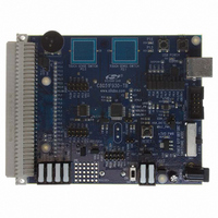
Manufacturer Part Number
C8051F930-TB
Description
BOARD TARGET/PROTO W/C8051F930
Manufacturer
Silicon Laboratories Inc
Type
MCUr
Specifications of C8051F930-TB
Contents
Board
Processor To Be Evaluated
C8051F930
Processor Series
C8051F9xx
Data Bus Width
8 bit
Interface Type
I2C, UART, SPI
Maximum Operating Temperature
+ 85 C
Minimum Operating Temperature
- 40 C
Operating Supply Voltage
0.9 V to 3.6 V
Lead Free Status / RoHS Status
Lead free / RoHS Compliant
For Use With/related Products
C8051F930
Lead Free Status / Rohs Status
Lead free / RoHS Compliant
Other names
336-1472


C8051F93x-C8051F92x
18.2. Power-Fail (VDD/DC+ Supply Monitor) Reset
C8051F93x-C8051F92x devices have a VDD/DC+ Supply Monitor that is enabled and selected as a reset
source after each power-on or power-fail reset. When enabled and selected as a reset source, any power
down transition or power irregularity that causes VDD/DC+ to drop below V
be driven low and the CIP-51 will be held in a reset state (see Figure 18.3). When VDD/DC+ returns to a
level above V
After a power-fail reset, the PORSF flag reads 1, the contents of RAM invalid, and the VDD/DC+ supply
monitor is enabled and selected as a reset source. The enable state of the VDD/DC+ supply monitor and
its selection as a reset source is only altered by power-on and power-fail resets. For example, if the
VDD/DC+ supply monitor is de-selected as a reset source and disabled by software, then a software reset
is performed, the VDD/DC+ supply monitor will remain disabled and de-selected after the reset.
In battery-operated systems, the contents of RAM can be preserved near the end of the battery’s usable
life if the device is placed in sleep mode prior to a power-fail reset occurring. When the device is in sleep
mode, the power-fail reset is automatically disabled and the contents of RAM are preserved as long as the
VBAT supply does not fall below V
above V
source select state of the VDD/DC+ supply monitor are restored to the value last set by the user.
To allow software early notification that a power failure is about to occur, the VDDOK bit is cleared when
the VDD/DC+ supply falls below the V
interrupt. See Section “12. Interrupt Handler” on page 133 for more details.
Important Note: To protect the integrity of Flash contents, the VDD/DC+ supply monitor must be
enabled and selected as a reset source if software contains routines which erase or write Flash
memory. If the VDD/DC+ supply monitor is not enabled, any erase or write performed on Flash memory
will cause a Flash Error device reset.
182
V
V
POR
V
WARN
POR
RST
VDDOK
SLEEP
while the user is replacing the battery. Upon waking from sleep mode, the enable and reset
RST
RST
, the CIP-51 will be released from the reset state.
Power-Fail Reset
Active Mode
Figure 18.3. Power-Fail Reset Timing Diagram
POR
VDD/DC+
WARN
VBAT
. A large capacitor can be used to hold the power supply voltage
threshold. The VDDOK bit can be configured to generate an
Rev. 1.1
RAM Retained - No Reset
Sleep Mode
RST
Note: W akeup signal
will cause the RST pin to
required after new
battery insertion
t
Related parts for C8051F930-TB
Image
Part Number
Description
Manufacturer
Datasheet
Request
R

Part Number:
Description:
SMD/C°/SINGLE-ENDED OUTPUT SILICON OSCILLATOR
Manufacturer:
Silicon Laboratories Inc
Part Number:
Description:
Manufacturer:
Silicon Laboratories Inc
Datasheet:
Part Number:
Description:
N/A N/A/SI4010 AES KEYFOB DEMO WITH LCD RX
Manufacturer:
Silicon Laboratories Inc
Datasheet:
Part Number:
Description:
N/A N/A/SI4010 SIMPLIFIED KEY FOB DEMO WITH LED RX
Manufacturer:
Silicon Laboratories Inc
Datasheet:
Part Number:
Description:
N/A/-40 TO 85 OC/EZLINK MODULE; F930/4432 HIGH BAND (REV E/B1)
Manufacturer:
Silicon Laboratories Inc
Part Number:
Description:
EZLink Module; F930/4432 Low Band (rev e/B1)
Manufacturer:
Silicon Laboratories Inc
Part Number:
Description:
I°/4460 10 DBM RADIO TEST CARD 434 MHZ
Manufacturer:
Silicon Laboratories Inc
Part Number:
Description:
I°/4461 14 DBM RADIO TEST CARD 868 MHZ
Manufacturer:
Silicon Laboratories Inc
Part Number:
Description:
I°/4463 20 DBM RFSWITCH RADIO TEST CARD 460 MHZ
Manufacturer:
Silicon Laboratories Inc
Part Number:
Description:
I°/4463 20 DBM RADIO TEST CARD 868 MHZ
Manufacturer:
Silicon Laboratories Inc
Part Number:
Description:
I°/4463 27 DBM RADIO TEST CARD 868 MHZ
Manufacturer:
Silicon Laboratories Inc
Part Number:
Description:
I°/4463 SKYWORKS 30 DBM RADIO TEST CARD 915 MHZ
Manufacturer:
Silicon Laboratories Inc
Part Number:
Description:
N/A N/A/-40 TO 85 OC/4463 RFMD 30 DBM RADIO TEST CARD 915 MHZ
Manufacturer:
Silicon Laboratories Inc
Part Number:
Description:
I°/4463 20 DBM RADIO TEST CARD 169 MHZ
Manufacturer:
Silicon Laboratories Inc