C8051F930-TB Silicon Laboratories Inc, C8051F930-TB Datasheet - Page 28
C8051F930-TB
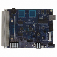
Manufacturer Part Number
C8051F930-TB
Description
BOARD TARGET/PROTO W/C8051F930
Manufacturer
Silicon Laboratories Inc
Type
MCUr
Specifications of C8051F930-TB
Contents
Board
Processor To Be Evaluated
C8051F930
Processor Series
C8051F9xx
Data Bus Width
8 bit
Interface Type
I2C, UART, SPI
Maximum Operating Temperature
+ 85 C
Minimum Operating Temperature
- 40 C
Operating Supply Voltage
0.9 V to 3.6 V
Lead Free Status / RoHS Status
Lead free / RoHS Compliant
For Use With/related Products
C8051F930
Lead Free Status / Rohs Status
Lead free / RoHS Compliant
Other names
336-1472


C8051F93x-C8051F92x
3.
28
*Note: Available only on the C8051F920/30.
XTAL3
XTAL4
DCEN
Name
C2CK
DC– /
VBAT
V
P2.7/
GND
GND
RST/
DC+
C2D
Pinout and Package Definitions
DD
/
‘F920/30 ‘F921/31
Table 3.1. Pin Definitions for the C8051F92x-C8051F93x
Pin Numbers
10
5
3
1
2
4
6
7
9
5
3
1
2
4
6
7
9
8
P Out
A Out
D I/O
D I/O
D I/O
D I/O
Type
P In
P In
P In
P In
A In
G
G
G
Description
Battery Supply Voltage. Must be 0.9 to 1.8 V in single-cell
battery mode and 1.8 to 3.6 V in dual-cell battery mode.
Power Supply Voltage. Must be 1.8 to 3.6 V. This supply
voltage is not required in low power sleep mode. This
voltage must always be > VBAT.
Positive output of the dc-dc converter. In single-cell battery
mode, a 1uF ceramic capacitor is required between DC+
and DC–. This pin can supply power to external devices
when operating in single-cell battery mode.
DC-DC converter return current path. In single-cell battery
mode, this pin is typically not connected to ground.
In dual-cell battery mode, this pin must be connected
directly to ground.
Required Ground.
DC-DC Enable Pin. In single-cell battery mode, this pin
must be connected to VBAT through a 0.68 µH inductor.
In dual-cell battery mode, this pin must be connected
directly to ground.
Device Reset. Open-drain output of internal POR or V
monitor. An external source can initiate a system reset by
driving this pin low for at least 15 µs. A 1 k to 5 k pullup
to V
complete description.
Clock signal for the C2 Debug Interface.
Port 2.7. This pin can only be used as GPIO. The Crossbar
cannot route signals to this pin and it cannot be configured
as an analog input. See Port I/O Section for a complete
description.
Bi-directional data signal for the C2 Debug Interface.
SmaRTClock Oscillator Crystal Input.
See Section 20 for a complete description.
SmaRTClock Oscillator Crystal Output.
See Section 20 for a complete description.
Rev. 1.1
DD
is recommended. See Reset Sources Section for a
DD
Related parts for C8051F930-TB
Image
Part Number
Description
Manufacturer
Datasheet
Request
R

Part Number:
Description:
SMD/C°/SINGLE-ENDED OUTPUT SILICON OSCILLATOR
Manufacturer:
Silicon Laboratories Inc
Part Number:
Description:
Manufacturer:
Silicon Laboratories Inc
Datasheet:
Part Number:
Description:
N/A N/A/SI4010 AES KEYFOB DEMO WITH LCD RX
Manufacturer:
Silicon Laboratories Inc
Datasheet:
Part Number:
Description:
N/A N/A/SI4010 SIMPLIFIED KEY FOB DEMO WITH LED RX
Manufacturer:
Silicon Laboratories Inc
Datasheet:
Part Number:
Description:
N/A/-40 TO 85 OC/EZLINK MODULE; F930/4432 HIGH BAND (REV E/B1)
Manufacturer:
Silicon Laboratories Inc
Part Number:
Description:
EZLink Module; F930/4432 Low Band (rev e/B1)
Manufacturer:
Silicon Laboratories Inc
Part Number:
Description:
I°/4460 10 DBM RADIO TEST CARD 434 MHZ
Manufacturer:
Silicon Laboratories Inc
Part Number:
Description:
I°/4461 14 DBM RADIO TEST CARD 868 MHZ
Manufacturer:
Silicon Laboratories Inc
Part Number:
Description:
I°/4463 20 DBM RFSWITCH RADIO TEST CARD 460 MHZ
Manufacturer:
Silicon Laboratories Inc
Part Number:
Description:
I°/4463 20 DBM RADIO TEST CARD 868 MHZ
Manufacturer:
Silicon Laboratories Inc
Part Number:
Description:
I°/4463 27 DBM RADIO TEST CARD 868 MHZ
Manufacturer:
Silicon Laboratories Inc
Part Number:
Description:
I°/4463 SKYWORKS 30 DBM RADIO TEST CARD 915 MHZ
Manufacturer:
Silicon Laboratories Inc
Part Number:
Description:
N/A N/A/-40 TO 85 OC/4463 RFMD 30 DBM RADIO TEST CARD 915 MHZ
Manufacturer:
Silicon Laboratories Inc
Part Number:
Description:
I°/4463 20 DBM RADIO TEST CARD 169 MHZ
Manufacturer:
Silicon Laboratories Inc