C8051F930-TB Silicon Laboratories Inc, C8051F930-TB Datasheet - Page 176
C8051F930-TB
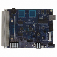
Manufacturer Part Number
C8051F930-TB
Description
BOARD TARGET/PROTO W/C8051F930
Manufacturer
Silicon Laboratories Inc
Type
MCUr
Specifications of C8051F930-TB
Contents
Board
Processor To Be Evaluated
C8051F930
Processor Series
C8051F9xx
Data Bus Width
8 bit
Interface Type
I2C, UART, SPI
Maximum Operating Temperature
+ 85 C
Minimum Operating Temperature
- 40 C
Operating Supply Voltage
0.9 V to 3.6 V
Lead Free Status / RoHS Status
Lead free / RoHS Compliant
For Use With/related Products
C8051F930
Lead Free Status / Rohs Status
Lead free / RoHS Compliant
Other names
336-1472


C8051F93x-C8051F92x
outputs during sleep mode, then the VDD/DC+ output can be made to float during Sleep mode by setting
the VDDSLP bit in the DC0CF register to 1.
Setting this bit can provide power savings in two ways. First, if the sleep interval is relatively short and the
VDD/DC+ load current (include leakage currents) is negligible, then the capacitor on VDD/DC+ will main-
tain the output voltage near the programmed value, which means that the VDD/DC+ capacitor will not need
to be recharged upon every wake up event. The second power advantage is that internal or external low-
power circuits that require more than 1.8 V can continue to function during Sleep mode without operating
the dc-dc converter, powered by the energy stored in the 1 µF output decoupling capacitor. For example,
the C8051F93x-C8051F92x comparators require about 0.4 µA when operating in their lowest power mode.
If the dc-dc converter output were increased to 3.3 V just before putting the device into Sleep mode, then
the comparator could be powered for more than 3 seconds before the output voltage dropped to 1.8 V. In
this example, the overall energy consumption would be much lower than if the dc-dc converter were kept
running to power the comparator.
If the load current on VDD/DC+ is high enough to discharge the VDD/DC+ capacitance to a voltage lower
than VBAT during the sleep interval, an internal diode will prevent VDD/DC+ from dropping more than a
few hundred millivolts below VBAT. There may be some additional leakage current from VBAT to ground
when the VDD/DC+ level falls below VBAT, but this leakage current should be small compared to the cur-
rent from VDD/DC+.
The amount of time that it takes for a device configured in one-cell mode to wake up from Sleep mode
depends on a number of factors, including the dc-dc converter clock speed, the settings of the SWSEL and
ILIMIT bits, the battery internal resistance, the load current, and the difference between the VBAT voltage
level and the programmed output voltage. The wake up time can be as short as 2 µs, though it is more
commonly in the range of 5 to 10 µs, and it can exceed 50 µs under extreme conditions.
See Section “14. Power Management” on page 146 for more information about sleep mode.
176
Rev. 1.1
Related parts for C8051F930-TB
Image
Part Number
Description
Manufacturer
Datasheet
Request
R

Part Number:
Description:
SMD/C°/SINGLE-ENDED OUTPUT SILICON OSCILLATOR
Manufacturer:
Silicon Laboratories Inc
Part Number:
Description:
Manufacturer:
Silicon Laboratories Inc
Datasheet:
Part Number:
Description:
N/A N/A/SI4010 AES KEYFOB DEMO WITH LCD RX
Manufacturer:
Silicon Laboratories Inc
Datasheet:
Part Number:
Description:
N/A N/A/SI4010 SIMPLIFIED KEY FOB DEMO WITH LED RX
Manufacturer:
Silicon Laboratories Inc
Datasheet:
Part Number:
Description:
N/A/-40 TO 85 OC/EZLINK MODULE; F930/4432 HIGH BAND (REV E/B1)
Manufacturer:
Silicon Laboratories Inc
Part Number:
Description:
EZLink Module; F930/4432 Low Band (rev e/B1)
Manufacturer:
Silicon Laboratories Inc
Part Number:
Description:
I°/4460 10 DBM RADIO TEST CARD 434 MHZ
Manufacturer:
Silicon Laboratories Inc
Part Number:
Description:
I°/4461 14 DBM RADIO TEST CARD 868 MHZ
Manufacturer:
Silicon Laboratories Inc
Part Number:
Description:
I°/4463 20 DBM RFSWITCH RADIO TEST CARD 460 MHZ
Manufacturer:
Silicon Laboratories Inc
Part Number:
Description:
I°/4463 20 DBM RADIO TEST CARD 868 MHZ
Manufacturer:
Silicon Laboratories Inc
Part Number:
Description:
I°/4463 27 DBM RADIO TEST CARD 868 MHZ
Manufacturer:
Silicon Laboratories Inc
Part Number:
Description:
I°/4463 SKYWORKS 30 DBM RADIO TEST CARD 915 MHZ
Manufacturer:
Silicon Laboratories Inc
Part Number:
Description:
N/A N/A/-40 TO 85 OC/4463 RFMD 30 DBM RADIO TEST CARD 915 MHZ
Manufacturer:
Silicon Laboratories Inc
Part Number:
Description:
I°/4463 20 DBM RADIO TEST CARD 169 MHZ
Manufacturer:
Silicon Laboratories Inc