C8051F930-TB Silicon Laboratories Inc, C8051F930-TB Datasheet - Page 57
C8051F930-TB
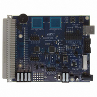
Manufacturer Part Number
C8051F930-TB
Description
BOARD TARGET/PROTO W/C8051F930
Manufacturer
Silicon Laboratories Inc
Type
MCUr
Specifications of C8051F930-TB
Contents
Board
Processor To Be Evaluated
C8051F930
Processor Series
C8051F9xx
Data Bus Width
8 bit
Interface Type
I2C, UART, SPI
Maximum Operating Temperature
+ 85 C
Minimum Operating Temperature
- 40 C
Operating Supply Voltage
0.9 V to 3.6 V
Lead Free Status / RoHS Status
Lead free / RoHS Compliant
For Use With/related Products
C8051F930
Lead Free Status / Rohs Status
Lead free / RoHS Compliant
Other names
336-1472


Table 4.4. Reset Electrical Characteristics
V
RST Output Low Voltage
RST Input High Voltage
RST Input Low Voltage
RST Input Pullup Current
VDD/DC+ Monitor Thresh-
old (V
VBAT Ramp Time for
Power On
VBAT Monitor Threshold
(V
Missing Clock Detector
Timeout
Minimum System Clock w/
Missing Clock Detector
Enabled
Reset Time Delay
Minimum RST Low Time to
Generate a System Reset
V
V
Current
DD
DD
DD
POR
= 1.8 to 3.6 V, –40 to +85 °C unless otherwise specified.
Monitor Turn-on Time
Monitor Supply
RST
)
Parameter
)
I
V
V
V
V
RST = 0.0 V, VDD = 1.8 V
RST = 0.0 V, VDD = 3.6 V
Early Warning
Reset Trigger
(all power modes except Sleep)
VBAT Ramp from 0–0.9 V
Initial Power-On (VBAT Rising)
Brownout Condition (VBAT Falling)
Recovery from Brownout (VBAT Rising)
Time from last system clock rising edge
to reset initiation
System clock frequency which triggers
a missing clock detector timeout
Delay between release of any reset
source and code
execution at location 0x0000
OL
DD
DD
DD
DD
= 1.4 mA,
= 2.0 to 3.6 V
= 0.9 to 2.0 V
= 2.0 to 3.6 V
= 0.9 to 2.0 V
Conditions
Rev. 1.1
C8051F93x-C8051F92x
V
0.7 x V
DD
Min
100
1.8
1.7
0.7
15
—
—
—
—
—
—
—
—
—
—
—
—
– 0.6
DD
1.85
1.75
0.75
0.95
Typ
650
300
0.8
—
—
—
—
—
20
—
10
—
4
7
7
0.3 x V
1000
Max
0.6
0.6
1.9
1.8
0.9
30
10
—
—
—
—
—
—
—
—
—
3
DD
Units
kHz
µA
ms
µA
µs
µs
µs
ns
V
V
V
V
V
V
V
57
Related parts for C8051F930-TB
Image
Part Number
Description
Manufacturer
Datasheet
Request
R

Part Number:
Description:
SMD/C°/SINGLE-ENDED OUTPUT SILICON OSCILLATOR
Manufacturer:
Silicon Laboratories Inc
Part Number:
Description:
Manufacturer:
Silicon Laboratories Inc
Datasheet:
Part Number:
Description:
N/A N/A/SI4010 AES KEYFOB DEMO WITH LCD RX
Manufacturer:
Silicon Laboratories Inc
Datasheet:
Part Number:
Description:
N/A N/A/SI4010 SIMPLIFIED KEY FOB DEMO WITH LED RX
Manufacturer:
Silicon Laboratories Inc
Datasheet:
Part Number:
Description:
N/A/-40 TO 85 OC/EZLINK MODULE; F930/4432 HIGH BAND (REV E/B1)
Manufacturer:
Silicon Laboratories Inc
Part Number:
Description:
EZLink Module; F930/4432 Low Band (rev e/B1)
Manufacturer:
Silicon Laboratories Inc
Part Number:
Description:
I°/4460 10 DBM RADIO TEST CARD 434 MHZ
Manufacturer:
Silicon Laboratories Inc
Part Number:
Description:
I°/4461 14 DBM RADIO TEST CARD 868 MHZ
Manufacturer:
Silicon Laboratories Inc
Part Number:
Description:
I°/4463 20 DBM RFSWITCH RADIO TEST CARD 460 MHZ
Manufacturer:
Silicon Laboratories Inc
Part Number:
Description:
I°/4463 20 DBM RADIO TEST CARD 868 MHZ
Manufacturer:
Silicon Laboratories Inc
Part Number:
Description:
I°/4463 27 DBM RADIO TEST CARD 868 MHZ
Manufacturer:
Silicon Laboratories Inc
Part Number:
Description:
I°/4463 SKYWORKS 30 DBM RADIO TEST CARD 915 MHZ
Manufacturer:
Silicon Laboratories Inc
Part Number:
Description:
N/A N/A/-40 TO 85 OC/4463 RFMD 30 DBM RADIO TEST CARD 915 MHZ
Manufacturer:
Silicon Laboratories Inc
Part Number:
Description:
I°/4463 20 DBM RADIO TEST CARD 169 MHZ
Manufacturer:
Silicon Laboratories Inc