C8051F930-TB Silicon Laboratories Inc, C8051F930-TB Datasheet - Page 9
C8051F930-TB
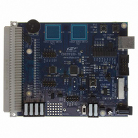
Manufacturer Part Number
C8051F930-TB
Description
BOARD TARGET/PROTO W/C8051F930
Manufacturer
Silicon Laboratories Inc
Type
MCUr
Specifications of C8051F930-TB
Contents
Board
Processor To Be Evaluated
C8051F930
Processor Series
C8051F9xx
Data Bus Width
8 bit
Interface Type
I2C, UART, SPI
Maximum Operating Temperature
+ 85 C
Minimum Operating Temperature
- 40 C
Operating Supply Voltage
0.9 V to 3.6 V
Lead Free Status / RoHS Status
Lead free / RoHS Compliant
For Use With/related Products
C8051F930
Lead Free Status / Rohs Status
Lead free / RoHS Compliant
Other names
336-1472


List of Figures
1. System Overview
2. Ordering Information
3. Pinout and Package Definitions
4. Electrical Characteristics
5. 10-Bit SAR ADC with 16-bit Auto-Averaging Accumulator and Autonomous Low
Figure 1.1. C8051F930 Block Diagram .................................................................... 19
Figure 1.2. C8051F931 Block Diagram .................................................................... 19
Figure 1.3. C8051F920 Block Diagram .................................................................... 20
Figure 1.4. C8051F921 Block Diagram .................................................................... 20
Figure 1.5. Port I/O Functional Block Diagram ......................................................... 22
Figure 1.6. PCA Block Diagram................................................................................ 23
Figure 1.7. ADC0 Functional Block Diagram............................................................ 24
Figure 1.8. ADC0 Multiplexer Block Diagram ........................................................... 25
Figure 1.9. Comparator 0 Functional Block Diagram ............................................... 26
Figure 1.10. Comparator 1 Functional Block Diagram ............................................. 26
Figure 3.1. QFN-32 Pinout Diagram (Top View) ...................................................... 32
Figure 3.2. QFN-24 Pinout Diagram (Top View) ...................................................... 33
Figure 3.3. LQFP-32 Pinout Diagram (Top View)..................................................... 34
Figure 3.4. QFN-32 Package Drawing ..................................................................... 35
Figure 3.5. Typical QFN-32 Landing Diagram.......................................................... 36
Figure 3.6. QFN-24 Package Drawing ..................................................................... 38
Figure 3.7. Typical QFN-24 Landing Diagram.......................................................... 39
Figure 3.8. LQFP-32 Package Diagram ................................................................... 41
Figure 3.9. Typical LQFP-32 Landing Diagram ........................................................ 42
Figure 4.1. Active Mode Current (External CMOS Clock) ........................................ 46
Figure 4.2. Idle Mode Current (External CMOS Clock) ............................................ 47
Figure 4.3. Typical DC-DC Converter Efficiency (High Current, VDD/DC+ = 2 V) ... 48
Figure 4.4. Typical DC-DC Converter Efficiency (High Current, VDD/DC+ = 3 V) ... 49
Figure 4.5. Typical DC-DC Converter Efficiency (Low Current, VDD/DC+ = 2 V).... 50
Figure 4.6. Typical One-Cell Suspend Mode Current............................................... 51
Figure 4.7. Typical VOH Curves, 1.8 – 3.6 V ........................................................... 53
Figure 4.8. Typical VOH Curves, 0.9 – 1.8 V ........................................................... 54
Figure 4.9. Typical VOL Curves, 1.8 – 3.6 V ............................................................ 55
Figure 4.10. Typical VOL Curves, 0.9 – 1.8 V .......................................................... 56
Figure 5.1. ADC0 Functional Block Diagram............................................................ 65
Figure 5.2. 10-Bit ADC Track and Conversion Example Timing (BURSTEN = 0).... 68
Figure 5.3. Burst Mode Tracking Example with Repeat Count Set to 4 ................... 69
Figure 5.4. ADC0 Equivalent Input Circuits .............................................................. 70
Figure 5.5. ADC Window Compare Example: Right-Justified Single-Ended Data ... 80
Figure 5.6. ADC Window Compare Example: Left-Justified Single-Ended Data...... 80
Figure 5.7. ADC0 Multiplexer Block Diagram ........................................................... 81
Figure 5.8. Temperature Sensor Transfer Function ................................................. 83
Power Burst Mode
Rev. 0.2
C8051F93x-C8051F92x
9
Related parts for C8051F930-TB
Image
Part Number
Description
Manufacturer
Datasheet
Request
R

Part Number:
Description:
SMD/C°/SINGLE-ENDED OUTPUT SILICON OSCILLATOR
Manufacturer:
Silicon Laboratories Inc
Part Number:
Description:
Manufacturer:
Silicon Laboratories Inc
Datasheet:
Part Number:
Description:
N/A N/A/SI4010 AES KEYFOB DEMO WITH LCD RX
Manufacturer:
Silicon Laboratories Inc
Datasheet:
Part Number:
Description:
N/A N/A/SI4010 SIMPLIFIED KEY FOB DEMO WITH LED RX
Manufacturer:
Silicon Laboratories Inc
Datasheet:
Part Number:
Description:
N/A/-40 TO 85 OC/EZLINK MODULE; F930/4432 HIGH BAND (REV E/B1)
Manufacturer:
Silicon Laboratories Inc
Part Number:
Description:
EZLink Module; F930/4432 Low Band (rev e/B1)
Manufacturer:
Silicon Laboratories Inc
Part Number:
Description:
I°/4460 10 DBM RADIO TEST CARD 434 MHZ
Manufacturer:
Silicon Laboratories Inc
Part Number:
Description:
I°/4461 14 DBM RADIO TEST CARD 868 MHZ
Manufacturer:
Silicon Laboratories Inc
Part Number:
Description:
I°/4463 20 DBM RFSWITCH RADIO TEST CARD 460 MHZ
Manufacturer:
Silicon Laboratories Inc
Part Number:
Description:
I°/4463 20 DBM RADIO TEST CARD 868 MHZ
Manufacturer:
Silicon Laboratories Inc
Part Number:
Description:
I°/4463 27 DBM RADIO TEST CARD 868 MHZ
Manufacturer:
Silicon Laboratories Inc
Part Number:
Description:
I°/4463 SKYWORKS 30 DBM RADIO TEST CARD 915 MHZ
Manufacturer:
Silicon Laboratories Inc
Part Number:
Description:
N/A N/A/-40 TO 85 OC/4463 RFMD 30 DBM RADIO TEST CARD 915 MHZ
Manufacturer:
Silicon Laboratories Inc
Part Number:
Description:
I°/4463 20 DBM RADIO TEST CARD 169 MHZ
Manufacturer:
Silicon Laboratories Inc