C8051F930-TB Silicon Laboratories Inc, C8051F930-TB Datasheet - Page 5
C8051F930-TB
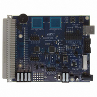
Manufacturer Part Number
C8051F930-TB
Description
BOARD TARGET/PROTO W/C8051F930
Manufacturer
Silicon Laboratories Inc
Type
MCUr
Specifications of C8051F930-TB
Contents
Board
Processor To Be Evaluated
C8051F930
Processor Series
C8051F9xx
Data Bus Width
8 bit
Interface Type
I2C, UART, SPI
Maximum Operating Temperature
+ 85 C
Minimum Operating Temperature
- 40 C
Operating Supply Voltage
0.9 V to 3.6 V
Lead Free Status / RoHS Status
Lead free / RoHS Compliant
For Use With/related Products
C8051F930
Lead Free Status / Rohs Status
Lead free / RoHS Compliant
Other names
336-1472


14. Power Management.............................................................................................. 156
15. Cyclic Redundancy Check Unit (CRC0) ............................................................. 164
16. On-Chip DC-DC Converter (DC0) ........................................................................ 171
17. Voltage Regulator (VREG0) ................................................................................. 179
18. Reset Sources....................................................................................................... 180
13.2.Non-volatile Data Storage .............................................................................. 147
13.3.Security Options ............................................................................................. 147
13.4.Determining the Device Part Number at Run Time ........................................ 149
13.5.Flash Write and Erase Guidelines .................................................................. 150
13.6.Minimizing Flash Read Current ...................................................................... 152
14.1.Normal Mode .................................................................................................. 157
14.2.Idle Mode........................................................................................................ 158
14.3.Stop Mode ...................................................................................................... 158
14.4.Suspend Mode ............................................................................................... 159
14.5.Sleep Mode .................................................................................................... 159
14.6.Configuring Wakeup Sources......................................................................... 160
14.7.Determining the Event that Caused the Last Wakeup.................................... 161
14.8.Power Management Specifications ................................................................ 163
15.1.CRC Algorithm................................................................................................ 164
15.2.Preparing for a CRC Calculation .................................................................... 166
15.3.Performing a CRC Calculation ....................................................................... 166
15.4.Accessing the CRC0 Result ........................................................................... 166
15.5.CRC0 Bit Reverse Feature............................................................................. 170
16.1.Startup Behavior............................................................................................. 172
16.2.High Power Applications................................................................................. 173
16.3.Pulse Skipping Mode...................................................................................... 173
16.4.Enabling the DC-DC Converter ...................................................................... 174
16.5.Minimizing Power Supply Noise ..................................................................... 175
16.6.Selecting the Optimum Switch Size................................................................ 175
16.7.DC-DC Converter Clocking Options ............................................................... 175
16.8.DC-DC Converter Behavior in Sleep Mode .................................................... 175
16.9.DC-DC Converter Register Descriptions ........................................................ 177
16.10.DC-DC Converter Specifications .................................................................. 178
17.1.Voltage Regulator Electrical Specifications .................................................... 179
18.1.Power-On (VBAT Supply Monitor) Reset ....................................................... 181
18.2.Power-Fail (VDD/DC+ Supply Monitor) Reset................................................ 182
18.3.External Reset ................................................................................................ 184
18.4.Missing Clock Detector Reset ........................................................................ 184
18.5.Comparator0 Reset ........................................................................................ 184
18.6.PCA Watchdog Timer Reset .......................................................................... 184
18.7.Flash Error Reset ........................................................................................... 185
13.1.3.Flash Write Procedure ........................................................................... 146
13.5.1.VDD Maintenance and the VDD Monitor ............................................... 150
13.5.2.PSWE Maintenance ............................................................................... 151
13.5.3.System Clock ......................................................................................... 151
Rev. 1.1
C8051F93x-C8051F92x
5
Related parts for C8051F930-TB
Image
Part Number
Description
Manufacturer
Datasheet
Request
R

Part Number:
Description:
SMD/C°/SINGLE-ENDED OUTPUT SILICON OSCILLATOR
Manufacturer:
Silicon Laboratories Inc
Part Number:
Description:
Manufacturer:
Silicon Laboratories Inc
Datasheet:
Part Number:
Description:
N/A N/A/SI4010 AES KEYFOB DEMO WITH LCD RX
Manufacturer:
Silicon Laboratories Inc
Datasheet:
Part Number:
Description:
N/A N/A/SI4010 SIMPLIFIED KEY FOB DEMO WITH LED RX
Manufacturer:
Silicon Laboratories Inc
Datasheet:
Part Number:
Description:
N/A/-40 TO 85 OC/EZLINK MODULE; F930/4432 HIGH BAND (REV E/B1)
Manufacturer:
Silicon Laboratories Inc
Part Number:
Description:
EZLink Module; F930/4432 Low Band (rev e/B1)
Manufacturer:
Silicon Laboratories Inc
Part Number:
Description:
I°/4460 10 DBM RADIO TEST CARD 434 MHZ
Manufacturer:
Silicon Laboratories Inc
Part Number:
Description:
I°/4461 14 DBM RADIO TEST CARD 868 MHZ
Manufacturer:
Silicon Laboratories Inc
Part Number:
Description:
I°/4463 20 DBM RFSWITCH RADIO TEST CARD 460 MHZ
Manufacturer:
Silicon Laboratories Inc
Part Number:
Description:
I°/4463 20 DBM RADIO TEST CARD 868 MHZ
Manufacturer:
Silicon Laboratories Inc
Part Number:
Description:
I°/4463 27 DBM RADIO TEST CARD 868 MHZ
Manufacturer:
Silicon Laboratories Inc
Part Number:
Description:
I°/4463 SKYWORKS 30 DBM RADIO TEST CARD 915 MHZ
Manufacturer:
Silicon Laboratories Inc
Part Number:
Description:
N/A N/A/-40 TO 85 OC/4463 RFMD 30 DBM RADIO TEST CARD 915 MHZ
Manufacturer:
Silicon Laboratories Inc
Part Number:
Description:
I°/4463 20 DBM RADIO TEST CARD 169 MHZ
Manufacturer:
Silicon Laboratories Inc