C8051F930-TB Silicon Laboratories Inc, C8051F930-TB Datasheet - Page 302
C8051F930-TB
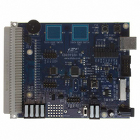
Manufacturer Part Number
C8051F930-TB
Description
BOARD TARGET/PROTO W/C8051F930
Manufacturer
Silicon Laboratories Inc
Type
MCUr
Specifications of C8051F930-TB
Contents
Board
Processor To Be Evaluated
C8051F930
Processor Series
C8051F9xx
Data Bus Width
8 bit
Interface Type
I2C, UART, SPI
Maximum Operating Temperature
+ 85 C
Minimum Operating Temperature
- 40 C
Operating Supply Voltage
0.9 V to 3.6 V
Lead Free Status / RoHS Status
Lead free / RoHS Compliant
For Use With/related Products
C8051F930
Lead Free Status / Rohs Status
Lead free / RoHS Compliant
Other names
336-1472


C8051F93x-C8051F92x
26.2. PCA0 Interrupt Sources
Figure 26.3 shows a diagram of the PCA interrupt tree. There are eight independent event flags that can
be used to generate a PCA0 interrupt. They are: the main PCA counter overflow flag (CF), which is set
upon a 16-bit overflow of the PCA0 counter, an intermediate overflow flag (COVF), which can be set on an
overflow from the 8th, 9th, 10th, or 11th bit of the PCA0 counter, and the individual flags for each PCA
channel (CCF0, CCF1, CCF2, CCF3, CCF4, and CCF5), which are set according to the operation mode of
that module. These event flags are always set when the trigger condition occurs. Each of these flags can
be individually selected to generate a PCA0 interrupt, using the corresponding interrupt enable flag (ECF
for CF, ECOV for COVF, and ECCFn for each CCFn). PCA0 interrupts must be globally enabled before any
individual interrupt sources are recognized by the processor. PCA0 interrupts are globally enabled by
setting the EA bit and the EPCA0 bit to logic 1.
302
PCA Counter/Timer 8, 9,
PCA Counter/Timer 16-
10 or 11-bit Overflow
bit Overflow
W
P
M
1
6
n
PCA Module 0
PCA Module 1
PCA Module 2
PCA Module 3
PCA Module 4
PCA Module 5
(for n = 0 to 5)
PCA0CPMn
O
M
E
C
n
C
A
P
P
(CCF0)
(CCF1)
(CCF2)
(CCF3)
(CCF4)
(CCF5)
n
C
A
P
N
n
M
A
T
n
O
G
T
n
W
M
P
n
E
C
C
F
n
C
F
C
R
PCA0CN
C
C
F
5
C
C
F
4
C
C
F
3
Figure 26.3. PCA Interrupt Block Diagram
C
C
F
2
C
C
F
1
C
C
F
0
ECCF0
ECCF1
ECCF2
ECCF3
ECCF4
ECCF5
C
D
L
I
W
D
T
E
PCA0MD
W
D
C
K
L
C
P
S
2
C
P
S
1
0
1
0
1
0
1
0
1
0
1
0
1
C
P
S
0
E
C
F
0
1
Rev. 1.1
A
R
S
E
L
C
O
V
PCA0PWM
F
C
O
E
V
0
1
C
S
E
L
L
1
C
L
S
E
L
0
Set 8, 9, 10, or 11 bit Operation
EPCA0
0
1
EA
0
1
Interrupt
Priority
Decoder
Related parts for C8051F930-TB
Image
Part Number
Description
Manufacturer
Datasheet
Request
R

Part Number:
Description:
SMD/C°/SINGLE-ENDED OUTPUT SILICON OSCILLATOR
Manufacturer:
Silicon Laboratories Inc
Part Number:
Description:
Manufacturer:
Silicon Laboratories Inc
Datasheet:
Part Number:
Description:
N/A N/A/SI4010 AES KEYFOB DEMO WITH LCD RX
Manufacturer:
Silicon Laboratories Inc
Datasheet:
Part Number:
Description:
N/A N/A/SI4010 SIMPLIFIED KEY FOB DEMO WITH LED RX
Manufacturer:
Silicon Laboratories Inc
Datasheet:
Part Number:
Description:
N/A/-40 TO 85 OC/EZLINK MODULE; F930/4432 HIGH BAND (REV E/B1)
Manufacturer:
Silicon Laboratories Inc
Part Number:
Description:
EZLink Module; F930/4432 Low Band (rev e/B1)
Manufacturer:
Silicon Laboratories Inc
Part Number:
Description:
I°/4460 10 DBM RADIO TEST CARD 434 MHZ
Manufacturer:
Silicon Laboratories Inc
Part Number:
Description:
I°/4461 14 DBM RADIO TEST CARD 868 MHZ
Manufacturer:
Silicon Laboratories Inc
Part Number:
Description:
I°/4463 20 DBM RFSWITCH RADIO TEST CARD 460 MHZ
Manufacturer:
Silicon Laboratories Inc
Part Number:
Description:
I°/4463 20 DBM RADIO TEST CARD 868 MHZ
Manufacturer:
Silicon Laboratories Inc
Part Number:
Description:
I°/4463 27 DBM RADIO TEST CARD 868 MHZ
Manufacturer:
Silicon Laboratories Inc
Part Number:
Description:
I°/4463 SKYWORKS 30 DBM RADIO TEST CARD 915 MHZ
Manufacturer:
Silicon Laboratories Inc
Part Number:
Description:
N/A N/A/-40 TO 85 OC/4463 RFMD 30 DBM RADIO TEST CARD 915 MHZ
Manufacturer:
Silicon Laboratories Inc
Part Number:
Description:
I°/4463 20 DBM RADIO TEST CARD 169 MHZ
Manufacturer:
Silicon Laboratories Inc