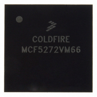
MCF5272VM66 Freescale Semiconductor, MCF5272VM66 Datasheet - Page 196

MCF5272VM66
Manufacturer Part Number
MCF5272VM66
Description
IC MPU 66MHZ COLDFIRE 196-MAPBGA
Manufacturer
Freescale Semiconductor
Series
MCF527xr
Specifications of MCF5272VM66
Core Processor
Coldfire V2
Core Size
32-Bit
Speed
66MHz
Connectivity
EBI/EMI, Ethernet, I²C, SPI, UART/USART, USB
Peripherals
DMA, WDT
Number Of I /o
32
Program Memory Size
16KB (4K x 32)
Program Memory Type
ROM
Ram Size
1K x 32
Voltage - Supply (vcc/vdd)
3 V ~ 3.6 V
Oscillator Type
External
Operating Temperature
0°C ~ 70°C
Package / Case
196-MAPBGA
Family Name
MCF5xxx
Device Core
ColdFire
Device Core Size
32b
Frequency (max)
66MHz
Instruction Set Architecture
RISC
Supply Voltage 1 (typ)
3.3V
Operating Temp Range
0C to 70C
Operating Temperature Classification
Commercial
Mounting
Surface Mount
Pin Count
196
Package Type
MA-BGA
Cpu Speed
66MHz
Embedded Interface Type
UART, QSPI, USB, TDM
Digital Ic Case Style
BGA
No. Of Pins
196
Supply Voltage Range
3V To 3.6V
Rohs Compliant
Yes
Lead Free Status / RoHS Status
Lead free / RoHS Compliant
Eeprom Size
-
Data Converters
-
Lead Free Status / Rohs Status
Compliant
Available stocks
Company
Part Number
Manufacturer
Quantity
Price
Company:
Part Number:
MCF5272VM66
Manufacturer:
FREESCAL
Quantity:
30 000
Company:
Part Number:
MCF5272VM66
Manufacturer:
MOTOLOLA
Quantity:
648
Company:
Part Number:
MCF5272VM66
Manufacturer:
Freescale Semiconductor
Quantity:
10 000
Part Number:
MCF5272VM66
Manufacturer:
MOTOROLA/摩托罗拉
Quantity:
20 000
Part Number:
MCF5272VM66 K75N
Manufacturer:
FREESCALE
Quantity:
20 000
Company:
Part Number:
MCF5272VM66J
Manufacturer:
FREESCAL
Quantity:
416
Company:
Part Number:
MCF5272VM66J
Manufacturer:
Freescale
Quantity:
178
Company:
Part Number:
MCF5272VM66J
Manufacturer:
Freescale Semiconductor
Quantity:
10 000
Company:
Part Number:
MCF5272VM66K75N
Manufacturer:
Freescal
Quantity:
18
Company:
Part Number:
MCF5272VM66R2
Manufacturer:
Freescale Semiconductor
Quantity:
10 000
Company:
Part Number:
MCF5272VM66R2J
Manufacturer:
Freescale Semiconductor
Quantity:
10 000
- Current page: 196 of 544
- Download datasheet (7Mb)
SDRAM Controller
9.4
SDRAMs can have up to four banks addressed by SDBA1 and SDBA0. The two uppermost address lines
of the memory space are mapped to SDBA1 and SDBA0. Specific address lines mapped depend on the
size of the SDRAM array and are defined in the SDCR.
Each of the four bank address registers holds the page address (lower bits of row address) of an activated
page. Each bank can have one open page. A device with two banks can have two open pages. A device
with four banks can have four open pages.
The lower addresses of the row address are compared against the page address register content. If it does
not match, the SDRAM controller precharges the open page on the accessed bank and activates the new
required page. After this, the SDRAM controller executes the
page address register of the bank is updated. This is called a page miss.
After a bank is activated, it remains activated until the next page access causing a page miss.
A precharge of a deactivated bank is allowed and simply ignored by the SDRAM.
If a memory access is to an open page only the
called a page hit.
In two-page SDRAMs, banks 2 and 3 are invalid and must not be addressed. To avoid address aliasing, the
user should restrict the chip select address range to the space available in the SDRAMs.
9.5
The SDRAM configuration register (SDCR) and the SDRAM timing register (SDTR) are described in the
following sections. Note that SDRAM provides a mode register that is not part of the SDRAM controller
memory model. The SDRAM mode register is automatically configured during initialization.
9.5.1
SDCR is used to configure the SDRAM controller address multiplexers for the type of SDRAM devices
used on the system board.
Table 9-7
9-6
Reset
Write
Addr
R/W
SDRAM Banks, Page Hits, and Page Misses
SDRAM Registers
describes SDCR fields.
SDRAM Configuration Register (SDCR)
15
—
0
14
MCAS
00
MCF5272 ColdFire
13
Figure 9-3. SDRAM Configuration Register (SDCR)
12
00
—
11
®
Integrated Microprocessor User’s Manual, Rev. 3
10
Read/Write
BALOC
001
READ
MBAR + 0x0182
8
or
WRITE
GSL
7
0
READ
command is issued to the SDRAM. This is
6
—
00
or
5
WRITE
REG
4
0
command. Concurrently, the
INV SLEEP ACT
1
3
Freescale Semiconductor
Read-only
2
0
0
1
INIT
R/W
0
0
Related parts for MCF5272VM66
Image
Part Number
Description
Manufacturer
Datasheet
Request
R
Part Number:
Description:
Mcf5272 Coldfire Integrated Microprocessor User
Manufacturer:
Freescale Semiconductor, Inc
Datasheet:

Part Number:
Description:
MCF5272 Interrupt Service Routine for the Physical Layer Interface Controller
Manufacturer:
Freescale Semiconductor / Motorola
Datasheet:
Part Number:
Description:
Manufacturer:
Freescale Semiconductor, Inc
Datasheet:
Part Number:
Description:
Manufacturer:
Freescale Semiconductor, Inc
Datasheet:
Part Number:
Description:
Manufacturer:
Freescale Semiconductor, Inc
Datasheet:
Part Number:
Description:
Manufacturer:
Freescale Semiconductor, Inc
Datasheet:
Part Number:
Description:
Manufacturer:
Freescale Semiconductor, Inc
Datasheet:
Part Number:
Description:
Manufacturer:
Freescale Semiconductor, Inc
Datasheet:
Part Number:
Description:
Manufacturer:
Freescale Semiconductor, Inc
Datasheet:
Part Number:
Description:
Manufacturer:
Freescale Semiconductor, Inc
Datasheet:
Part Number:
Description:
Manufacturer:
Freescale Semiconductor, Inc
Datasheet:
Part Number:
Description:
Manufacturer:
Freescale Semiconductor, Inc
Datasheet:
Part Number:
Description:
Manufacturer:
Freescale Semiconductor, Inc
Datasheet:
Part Number:
Description:
Manufacturer:
Freescale Semiconductor, Inc
Datasheet:
Part Number:
Description:
Manufacturer:
Freescale Semiconductor, Inc
Datasheet:


