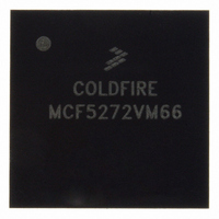
MCF5272VM66 Freescale Semiconductor, MCF5272VM66 Datasheet - Page 205

MCF5272VM66
Manufacturer Part Number
MCF5272VM66
Description
IC MPU 66MHZ COLDFIRE 196-MAPBGA
Manufacturer
Freescale Semiconductor
Series
MCF527xr
Specifications of MCF5272VM66
Core Processor
Coldfire V2
Core Size
32-Bit
Speed
66MHz
Connectivity
EBI/EMI, Ethernet, I²C, SPI, UART/USART, USB
Peripherals
DMA, WDT
Number Of I /o
32
Program Memory Size
16KB (4K x 32)
Program Memory Type
ROM
Ram Size
1K x 32
Voltage - Supply (vcc/vdd)
3 V ~ 3.6 V
Oscillator Type
External
Operating Temperature
0°C ~ 70°C
Package / Case
196-MAPBGA
Family Name
MCF5xxx
Device Core
ColdFire
Device Core Size
32b
Frequency (max)
66MHz
Instruction Set Architecture
RISC
Supply Voltage 1 (typ)
3.3V
Operating Temp Range
0C to 70C
Operating Temperature Classification
Commercial
Mounting
Surface Mount
Pin Count
196
Package Type
MA-BGA
Cpu Speed
66MHz
Embedded Interface Type
UART, QSPI, USB, TDM
Digital Ic Case Style
BGA
No. Of Pins
196
Supply Voltage Range
3V To 3.6V
Rohs Compliant
Yes
Lead Free Status / RoHS Status
Lead free / RoHS Compliant
Eeprom Size
-
Data Converters
-
Lead Free Status / Rohs Status
Compliant
Available stocks
Company
Part Number
Manufacturer
Quantity
Price
Company:
Part Number:
MCF5272VM66
Manufacturer:
FREESCAL
Quantity:
30 000
Company:
Part Number:
MCF5272VM66
Manufacturer:
MOTOLOLA
Quantity:
648
Company:
Part Number:
MCF5272VM66
Manufacturer:
Freescale Semiconductor
Quantity:
10 000
Part Number:
MCF5272VM66
Manufacturer:
MOTOROLA/摩托罗拉
Quantity:
20 000
Part Number:
MCF5272VM66 K75N
Manufacturer:
FREESCALE
Quantity:
20 000
Company:
Part Number:
MCF5272VM66J
Manufacturer:
FREESCAL
Quantity:
416
Company:
Part Number:
MCF5272VM66J
Manufacturer:
Freescale
Quantity:
178
Company:
Part Number:
MCF5272VM66J
Manufacturer:
Freescale Semiconductor
Quantity:
10 000
Company:
Part Number:
MCF5272VM66K75N
Manufacturer:
Freescal
Quantity:
18
Company:
Part Number:
MCF5272VM66R2
Manufacturer:
Freescale Semiconductor
Quantity:
10 000
Company:
Part Number:
MCF5272VM66R2J
Manufacturer:
Freescale Semiconductor
Quantity:
10 000
- Current page: 205 of 544
- Download datasheet (7Mb)
The controller allows single-beat read/write accesses and the following burst accesses:
These SDRAM accesses are shown in
low-power, self-refreshing sleep mode as shown in
off the SDRAM controller completely using the power management control register in the SIM.
Figures show burst read and burst writes, with a page miss and a page hit for each case. A single-cycle read
or write is identical to the first access of a burst. In normal operation the SDRAM controller refreshes the
SDRAM.
As these examples show, SDCLKE is normally high and SDCLK is always active. SDCLKE can be forced
to 0 and SDCLK can be shut off by putting the SDRAM controller into power down or self-refresh mode.
9.10.1
The read examples,
SDCR[INV] = 1.
In T1, the ColdFire core issues the address. This cycle is internal to the device and always occurs. In T2,
the SDRAM controller determines if there is a page miss or hit. This cycle is internal to the device and
always occurs.
Because
During precharge the SDRAM writes the designated on-chip RAM page buffer back into the SDRAM
array. The number of cycles for a precharge is set by programming SDTR[RP]. The default after reset is
two cycles. The activate new page cycle that follows (T5) is required to open a new page due to the page
miss. Cycle T6 is a wait state for SDRAM activation command. It is added due to default value of 0b01 in
SDTR[RCD]. For lower clock speed systems the RCD value could be written as 00 and this clock cycle
can be removed. Consult the data sheets of the SDRAM devices being used.
Freescale Semiconductor
•
•
•
16-byte cache line read bursts from 32-bit wide SDRAM with access times of n-1-1-1. The value
of n depends on read, write, page miss, page hit, etc. The enable extended bursts bit in chip select
option register 7 (CSOR7[EXTBURST]) must be cleared, CSBR7[EBI] must be set for SDRAM,
and CSBR7[BW] must be set for a 16-byte cache line width.
16-byte cache line read bursts from 16-bit wide SDRAM with access times of n-1-1-1-1-1-1-1.
CSOR7[EXTBURST] must be set, CSBR7[EBI] must be set for SDRAM, and CSBR7[BW] must
be set for 16 bits.
16-byte read or write bursts during Ethernet DMA transfers to/from SDRAM with access times of
n-1-1-1 or n-1-1-1-1-1-1-1 depending on 32 or 16 bit SDRAM port width as described in the
previous two paragraphs.
Figure 9-9
SDRAM Read Accesses
The SDRAM shares address and data signals with external memory and
peripherals. Due to stringent SDRAM timing requirements, it is strongly
recommended to buffer the address, byte strobe, and data buses between the
MCF5272 and non-SDRAM memory and peripherals. Never buffer signals
to the SDRAMs. See Appendix C for details on how to buffer external
memory and peripherals in a system using SDRAM.
shows a page miss, the
Figure 9-9
MCF5272 ColdFire
and
Figure
®
Figure 9-9
Integrated Microprocessor User’s Manual, Rev. 3
9-10, show a CAS latency of 2, SDCR[REG] = 0 and
PRECHARGE
NOTE
through
Figure 9-14
command (T3) and the following cycle occur.
Figure
and
9-15. The SDRAM supports a
Figure
9-15. It is also possible to turn
SDRAM Controller
9-15
Related parts for MCF5272VM66
Image
Part Number
Description
Manufacturer
Datasheet
Request
R
Part Number:
Description:
Mcf5272 Coldfire Integrated Microprocessor User
Manufacturer:
Freescale Semiconductor, Inc
Datasheet:

Part Number:
Description:
MCF5272 Interrupt Service Routine for the Physical Layer Interface Controller
Manufacturer:
Freescale Semiconductor / Motorola
Datasheet:
Part Number:
Description:
Manufacturer:
Freescale Semiconductor, Inc
Datasheet:
Part Number:
Description:
Manufacturer:
Freescale Semiconductor, Inc
Datasheet:
Part Number:
Description:
Manufacturer:
Freescale Semiconductor, Inc
Datasheet:
Part Number:
Description:
Manufacturer:
Freescale Semiconductor, Inc
Datasheet:
Part Number:
Description:
Manufacturer:
Freescale Semiconductor, Inc
Datasheet:
Part Number:
Description:
Manufacturer:
Freescale Semiconductor, Inc
Datasheet:
Part Number:
Description:
Manufacturer:
Freescale Semiconductor, Inc
Datasheet:
Part Number:
Description:
Manufacturer:
Freescale Semiconductor, Inc
Datasheet:
Part Number:
Description:
Manufacturer:
Freescale Semiconductor, Inc
Datasheet:
Part Number:
Description:
Manufacturer:
Freescale Semiconductor, Inc
Datasheet:
Part Number:
Description:
Manufacturer:
Freescale Semiconductor, Inc
Datasheet:
Part Number:
Description:
Manufacturer:
Freescale Semiconductor, Inc
Datasheet:
Part Number:
Description:
Manufacturer:
Freescale Semiconductor, Inc
Datasheet:


