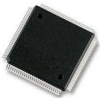
S9S12HZ128J3VAL Freescale Semiconductor, S9S12HZ128J3VAL Datasheet - Page 142

S9S12HZ128J3VAL
Manufacturer Part Number
S9S12HZ128J3VAL
Description
IC MCU FLASH 112-LQFP
Manufacturer
Freescale Semiconductor
Series
HCS12r
Datasheet
1.S9S12HZ128J3VAL.pdf
(692 pages)
Specifications of S9S12HZ128J3VAL
Core Processor
HCS12
Core Size
16-Bit
Speed
25MHz
Connectivity
CAN, EBI/EMI, I²C, SCI, SPI
Peripherals
LCD, Motor control PWM, POR, PWM, WDT
Number Of I /o
91
Program Memory Size
128KB (128K x 8)
Program Memory Type
FLASH
Eeprom Size
2K x 8
Ram Size
6K x 8
Voltage - Supply (vcc/vdd)
2.35 V ~ 2.75 V
Data Converters
A/D 16x10b
Oscillator Type
Internal
Operating Temperature
-40°C ~ 105°C
Package / Case
112-LQFP
Processor Series
S12HY
Core
HCS12X
Data Bus Width
16 bit
Data Ram Size
6 KB
Interface Type
CAN, I2C, SCI, SPI
Maximum Clock Frequency
50 MHz
Number Of Programmable I/os
85
Number Of Timers
1
Operating Supply Voltage
4.5 V to 5.5 V
Maximum Operating Temperature
+ 105 C
Mounting Style
SMD/SMT
Lead Free Status / RoHS Status
Lead free / RoHS Compliant
Available stocks
Company
Part Number
Manufacturer
Quantity
Price
Company:
Part Number:
S9S12HZ128J3VAL
Manufacturer:
Freescale Semiconductor
Quantity:
10 000
Part Number:
S9S12HZ128J3VAL
Manufacturer:
FREESCALE
Quantity:
20 000
Part Number:
S9S12HZ128J3VAL(MC9S12HZ128VAL
Manufacturer:
FREESCALE
Quantity:
20 000
- Current page: 142 of 692
- Download datasheet (4Mb)
Chapter 4 Port Integration Module (PIM9HZ256V2)
4.3.4.7
Read: Anytime. Write: Anytime.
This register selects whether a port P output is configured as push-pull or wired-or. When a Wired-OR
Mode Register bit is set to 1, the corresponding output pin is driven active low only (open drain) and a
high level is not driven. A Wired-OR Mode Register bit has no effect if the corresponding pin is configured
as an input.
If the IIC is enabled and the corresponding PWM channels are disabled, the PP[5:4] pins are configured
as wired-or and the corresponding Wired-OR Mode Register bits have no effect.
142
WOMP[5:4]
WOMP2
WOMP0
Reset
Field
5:4
2
0
W
R
Wired-OR Mode Port P
0 Output buffers operate as push-pull outputs.
1 Output buffers operate as open-drain outputs.
Wired-OR Mode Port P
0 Output buffers operate as push-pull outputs.
1 Output buffers operate as open-drain outputs.
Wired-OR Mode Port P
0 Output buffers operate as push-pull outputs.
1 Output buffers operate as open-drain outputs.
Port P Wired-OR Mode Register (WOMP)
0
0
7
= Reserved or Unimplemented
0
0
6
Figure 4-29. Port P Wired-OR Mode Register (WOMP)
Table 4-22. WOMP Field Descriptions
WOMP5
MC9S12HZ256 Data Sheet, Rev. 2.05
0
5
WOMP4
0
4
Description
0
0
3
WOMP2
0
2
Freescale Semiconductor
0
0
1
WOMPO
0
0
Related parts for S9S12HZ128J3VAL
Image
Part Number
Description
Manufacturer
Datasheet
Request
R
Part Number:
Description:
Manufacturer:
Freescale Semiconductor, Inc
Datasheet:
Part Number:
Description:
Manufacturer:
Freescale Semiconductor, Inc
Datasheet:
Part Number:
Description:
Manufacturer:
Freescale Semiconductor, Inc
Datasheet:
Part Number:
Description:
Manufacturer:
Freescale Semiconductor, Inc
Datasheet:
Part Number:
Description:
Manufacturer:
Freescale Semiconductor, Inc
Datasheet:
Part Number:
Description:
Manufacturer:
Freescale Semiconductor, Inc
Datasheet:
Part Number:
Description:
Manufacturer:
Freescale Semiconductor, Inc
Datasheet:
Part Number:
Description:
Manufacturer:
Freescale Semiconductor, Inc
Datasheet:
Part Number:
Description:
Manufacturer:
Freescale Semiconductor, Inc
Datasheet:
Part Number:
Description:
Manufacturer:
Freescale Semiconductor, Inc
Datasheet:
Part Number:
Description:
Manufacturer:
Freescale Semiconductor, Inc
Datasheet:
Part Number:
Description:
Manufacturer:
Freescale Semiconductor, Inc
Datasheet:
Part Number:
Description:
Manufacturer:
Freescale Semiconductor, Inc
Datasheet:
Part Number:
Description:
Manufacturer:
Freescale Semiconductor, Inc
Datasheet:
Part Number:
Description:
Manufacturer:
Freescale Semiconductor, Inc
Datasheet:


