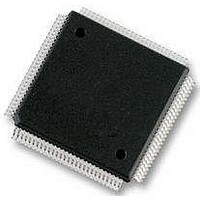
S9S12HZ128J3VAL Freescale Semiconductor, S9S12HZ128J3VAL Datasheet - Page 241

S9S12HZ128J3VAL
Manufacturer Part Number
S9S12HZ128J3VAL
Description
IC MCU FLASH 112-LQFP
Manufacturer
Freescale Semiconductor
Series
HCS12r
Datasheet
1.S9S12HZ128J3VAL.pdf
(692 pages)
Specifications of S9S12HZ128J3VAL
Core Processor
HCS12
Core Size
16-Bit
Speed
25MHz
Connectivity
CAN, EBI/EMI, I²C, SCI, SPI
Peripherals
LCD, Motor control PWM, POR, PWM, WDT
Number Of I /o
91
Program Memory Size
128KB (128K x 8)
Program Memory Type
FLASH
Eeprom Size
2K x 8
Ram Size
6K x 8
Voltage - Supply (vcc/vdd)
2.35 V ~ 2.75 V
Data Converters
A/D 16x10b
Oscillator Type
Internal
Operating Temperature
-40°C ~ 105°C
Package / Case
112-LQFP
Processor Series
S12HY
Core
HCS12X
Data Bus Width
16 bit
Data Ram Size
6 KB
Interface Type
CAN, I2C, SCI, SPI
Maximum Clock Frequency
50 MHz
Number Of Programmable I/os
85
Number Of Timers
1
Operating Supply Voltage
4.5 V to 5.5 V
Maximum Operating Temperature
+ 105 C
Mounting Style
SMD/SMT
Lead Free Status / RoHS Status
Lead free / RoHS Compliant
Available stocks
Company
Part Number
Manufacturer
Quantity
Price
Company:
Part Number:
S9S12HZ128J3VAL
Manufacturer:
Freescale Semiconductor
Quantity:
10 000
Part Number:
S9S12HZ128J3VAL
Manufacturer:
FREESCALE
Quantity:
20 000
Part Number:
S9S12HZ128J3VAL(MC9S12HZ128VAL
Manufacturer:
FREESCALE
Quantity:
20 000
- Current page: 241 of 692
- Download datasheet (4Mb)
Chapter 8
Liquid Crystal Display (LCD32F4BV1)
8.1
The LCD32F4B driver module has 32 frontplane drivers and 4 backplane drivers so that a maximum of
128 LCD segments are controllable. Each segment is controlled by a corresponding bit in the LCD RAM.
Four multiplex modes (1/1, 1/2, 1/3, 1/4 duty), and three bias (1/1, 1/2, 1/3) methods are available. The V
voltage is the lowest level of the output waveform and V
backplane pins can be multiplexed with other port functions.
The LCD32F4B driver system consists of five major sub-modules:
8.1.1
The LCD32F4B includes these distinctive features:
8.1.2
The LCD32F4B module supports five operation modes with different numbers of backplanes and different
biasing levels. During pseudo stop mode and wait mode the LCD operation can be suspended under
Freescale Semiconductor
•
•
•
•
•
•
•
•
•
•
•
Timing and Control – consists of registers and control logic for frame clock generation, bias
voltage level select, frame duty select, backplane select, and frontplane select/enable to produce
the required frame frequency and voltage waveforms.
LCD RAM – contains the data to be displayed on the LCD. Data can be read from or written to the
display RAM at any time.
Frontplane Drivers – consists of 32 frontplane drivers.
Backplane Drivers – consists of 4 backplane drivers.
Voltage Generator – Based on voltage applied to VLCD, it generates the voltage levels for the
timing and control logic to produce the frontplane and backplane waveforms.
Supports five LCD operation modes
32 frontplane drivers
4 backplane drivers
— Each frontplane has an enable bit respectively
Programmable frame clock generator
Programmable bias voltage level selector
On-chip generation of 4 different output voltage levels
Introduction
Features
Modes of Operation
MC9S12HZ256 Data Sheet, Rev. 2.05
3
becomes the highest level. All frontplane and
241
0
Related parts for S9S12HZ128J3VAL
Image
Part Number
Description
Manufacturer
Datasheet
Request
R
Part Number:
Description:
Manufacturer:
Freescale Semiconductor, Inc
Datasheet:
Part Number:
Description:
Manufacturer:
Freescale Semiconductor, Inc
Datasheet:
Part Number:
Description:
Manufacturer:
Freescale Semiconductor, Inc
Datasheet:
Part Number:
Description:
Manufacturer:
Freescale Semiconductor, Inc
Datasheet:
Part Number:
Description:
Manufacturer:
Freescale Semiconductor, Inc
Datasheet:
Part Number:
Description:
Manufacturer:
Freescale Semiconductor, Inc
Datasheet:
Part Number:
Description:
Manufacturer:
Freescale Semiconductor, Inc
Datasheet:
Part Number:
Description:
Manufacturer:
Freescale Semiconductor, Inc
Datasheet:
Part Number:
Description:
Manufacturer:
Freescale Semiconductor, Inc
Datasheet:
Part Number:
Description:
Manufacturer:
Freescale Semiconductor, Inc
Datasheet:
Part Number:
Description:
Manufacturer:
Freescale Semiconductor, Inc
Datasheet:
Part Number:
Description:
Manufacturer:
Freescale Semiconductor, Inc
Datasheet:
Part Number:
Description:
Manufacturer:
Freescale Semiconductor, Inc
Datasheet:
Part Number:
Description:
Manufacturer:
Freescale Semiconductor, Inc
Datasheet:
Part Number:
Description:
Manufacturer:
Freescale Semiconductor, Inc
Datasheet:


