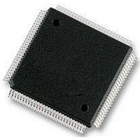
S9S12HZ128J3VAL Freescale Semiconductor, S9S12HZ128J3VAL Datasheet - Page 651

S9S12HZ128J3VAL
Manufacturer Part Number
S9S12HZ128J3VAL
Description
IC MCU FLASH 112-LQFP
Manufacturer
Freescale Semiconductor
Series
HCS12r
Datasheet
1.S9S12HZ128J3VAL.pdf
(692 pages)
Specifications of S9S12HZ128J3VAL
Core Processor
HCS12
Core Size
16-Bit
Speed
25MHz
Connectivity
CAN, EBI/EMI, I²C, SCI, SPI
Peripherals
LCD, Motor control PWM, POR, PWM, WDT
Number Of I /o
91
Program Memory Size
128KB (128K x 8)
Program Memory Type
FLASH
Eeprom Size
2K x 8
Ram Size
6K x 8
Voltage - Supply (vcc/vdd)
2.35 V ~ 2.75 V
Data Converters
A/D 16x10b
Oscillator Type
Internal
Operating Temperature
-40°C ~ 105°C
Package / Case
112-LQFP
Processor Series
S12HY
Core
HCS12X
Data Bus Width
16 bit
Data Ram Size
6 KB
Interface Type
CAN, I2C, SCI, SPI
Maximum Clock Frequency
50 MHz
Number Of Programmable I/os
85
Number Of Timers
1
Operating Supply Voltage
4.5 V to 5.5 V
Maximum Operating Temperature
+ 105 C
Mounting Style
SMD/SMT
Lead Free Status / RoHS Status
Lead free / RoHS Compliant
Available stocks
Company
Part Number
Manufacturer
Quantity
Price
Company:
Part Number:
S9S12HZ128J3VAL
Manufacturer:
Freescale Semiconductor
Quantity:
10 000
Part Number:
S9S12HZ128J3VAL
Manufacturer:
FREESCALE
Quantity:
20 000
Part Number:
S9S12HZ128J3VAL(MC9S12HZ128VAL
Manufacturer:
FREESCALE
Quantity:
20 000
- Current page: 651 of 692
- Download datasheet (4Mb)
A.8
A.9
A timing diagram of the external multiplexed-bus is illustrated in
values shown on table
write and data read cycle are shown, only one or the other would occur on a particular bus cycle.
The expanded bus timings are highly dependent on the load conditions. The timing parameters shown
assume a balanced load across all outputs.
Freescale Semiconductor
Conditions are shown in
Num C
10
11
12
1
1
2
3
4
5
6
7
8
9
1
2
LCD Supply Voltage
LCD Output Impedance(BP[3:0],FP[31:0])
for outputs to charge to higher voltage level or to
GND
LCD Output Current (BP[3:0],FP[31:0])
for outputs to discharge to lower voltage level
except GND
Outputs measured one at a time, low impedance voltage source connected to the VLCD pin.
Outputs measured one at a time, low impedance voltage source connected to the VLCD pin.
P Operating Frequency
P SCK Period t
D Enable Lead Time
D Enable Lag Time
D Clock (SCK) High or Low Time
D Data Setup Time (Inputs)
D Data Hold Time (Inputs)
D Slave Access Time
D Slave MISO Disable Time
D Data Valid (after SCK Edge)
D Data Hold Time (Outputs)
D Rise Time Inputs and Outputs
D Fall Time Inputs and Outputs
1
LCD_32F4B
External Bus Timing
2
Characteristic
sck
Table A-4
Table
= 1./f
Table A-21. LCD_32F4B Driver Electrical Characteristics
op
Table A-20. SPI Slave Mode Timing Characteristics
Rating
A-22. All major bus signals are included in the diagram. While both a data
unless otherwise noted, CLOAD = 200pF on all outputs
MC9S12HZ256 Data Sheet, Rev. 2.05
Symbol
Z
VLCD
I
BP/FP
BP/FP
Symbol
t
t
t
wsck
t
lead
t
f
t
t
sck
lag
t
t
dis
t
op
su
ho
t
t
hi
a
v
r
f
-0.25
Min.
50
-
Figure A-10
t
cyc
Min
DC
25
25
4
1
1
0
30
Typ.
-
-
-
Appendix A Electrical Characteristics
with the actual timing
Typ
VDDX + 0.25
Max.
5.0
-
2048
Max
1 4
25
25
25
1
1
Unit
k
uA
V
Unit
f
t
t
t
t
t
bus
bus
ns
ns
ns
ns
ns
ns
ns
cyc
cyc
cyc
cyc
651
Related parts for S9S12HZ128J3VAL
Image
Part Number
Description
Manufacturer
Datasheet
Request
R
Part Number:
Description:
Manufacturer:
Freescale Semiconductor, Inc
Datasheet:
Part Number:
Description:
Manufacturer:
Freescale Semiconductor, Inc
Datasheet:
Part Number:
Description:
Manufacturer:
Freescale Semiconductor, Inc
Datasheet:
Part Number:
Description:
Manufacturer:
Freescale Semiconductor, Inc
Datasheet:
Part Number:
Description:
Manufacturer:
Freescale Semiconductor, Inc
Datasheet:
Part Number:
Description:
Manufacturer:
Freescale Semiconductor, Inc
Datasheet:
Part Number:
Description:
Manufacturer:
Freescale Semiconductor, Inc
Datasheet:
Part Number:
Description:
Manufacturer:
Freescale Semiconductor, Inc
Datasheet:
Part Number:
Description:
Manufacturer:
Freescale Semiconductor, Inc
Datasheet:
Part Number:
Description:
Manufacturer:
Freescale Semiconductor, Inc
Datasheet:
Part Number:
Description:
Manufacturer:
Freescale Semiconductor, Inc
Datasheet:
Part Number:
Description:
Manufacturer:
Freescale Semiconductor, Inc
Datasheet:
Part Number:
Description:
Manufacturer:
Freescale Semiconductor, Inc
Datasheet:
Part Number:
Description:
Manufacturer:
Freescale Semiconductor, Inc
Datasheet:
Part Number:
Description:
Manufacturer:
Freescale Semiconductor, Inc
Datasheet:


