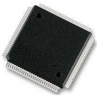
S9S12HZ128J3VAL Freescale Semiconductor, S9S12HZ128J3VAL Datasheet - Page 169

S9S12HZ128J3VAL
Manufacturer Part Number
S9S12HZ128J3VAL
Description
IC MCU FLASH 112-LQFP
Manufacturer
Freescale Semiconductor
Series
HCS12r
Datasheet
1.S9S12HZ128J3VAL.pdf
(692 pages)
Specifications of S9S12HZ128J3VAL
Core Processor
HCS12
Core Size
16-Bit
Speed
25MHz
Connectivity
CAN, EBI/EMI, I²C, SCI, SPI
Peripherals
LCD, Motor control PWM, POR, PWM, WDT
Number Of I /o
91
Program Memory Size
128KB (128K x 8)
Program Memory Type
FLASH
Eeprom Size
2K x 8
Ram Size
6K x 8
Voltage - Supply (vcc/vdd)
2.35 V ~ 2.75 V
Data Converters
A/D 16x10b
Oscillator Type
Internal
Operating Temperature
-40°C ~ 105°C
Package / Case
112-LQFP
Processor Series
S12HY
Core
HCS12X
Data Bus Width
16 bit
Data Ram Size
6 KB
Interface Type
CAN, I2C, SCI, SPI
Maximum Clock Frequency
50 MHz
Number Of Programmable I/os
85
Number Of Timers
1
Operating Supply Voltage
4.5 V to 5.5 V
Maximum Operating Temperature
+ 105 C
Mounting Style
SMD/SMT
Lead Free Status / RoHS Status
Lead free / RoHS Compliant
Available stocks
Company
Part Number
Manufacturer
Quantity
Price
Company:
Part Number:
S9S12HZ128J3VAL
Manufacturer:
Freescale Semiconductor
Quantity:
10 000
Part Number:
S9S12HZ128J3VAL
Manufacturer:
FREESCALE
Quantity:
20 000
Part Number:
S9S12HZ128J3VAL(MC9S12HZ128VAL
Manufacturer:
FREESCALE
Quantity:
20 000
- Current page: 169 of 692
- Download datasheet (4Mb)
5.2
This section lists and describes the signals that connect off chip.
5.2.1
These pins provides operating voltage (V
the supply voltage to the PLL to be independently bypassed. Even if PLL usage is not required V
and V
5.2.2
A passive external loop filter must be placed on the XFC pin. The filter is a second-order, low-pass filter
to eliminate the VCO input ripple. The value of the external filter network and the reference frequency
determines the speed of the corrections and the stability of the PLL. Refer to the device overview chapter
for calculation of PLL loop filter (XFC) components. If PLL usage is not required the XFC pin must be
tied to V
Freescale Semiconductor
1
Refer to the device overview section for availability of the low-voltage reset feature.
SSPLL
XCLKS
EXTAL
XTAL
DDPLL
External Signal Description
RESET
V
V
V
XFC — PLL Loop Filter Pin
must be connected properly.
XFC
DDPLL
SSPLL
DDPLL
Regulator
Monitor
Oscil-
.
Voltage
Clock
lator
, V
SSPLL
OSCCLK
PLL
CRG
Power-on Reset
Low Voltage Reset
— PLL Operating Voltage, PLL Ground
MC9S12HZ256 Data Sheet, Rev. 2.05
PLLCLK
Figure 5-1. CRG Block Diagram
CM fail
DDPLL
) and ground (V
Clock and Reset
1
Clock Quality
COP
Registers
Control
Checker
Generator
Reset
SSPLL
RTI
Chapter 5 Clocks and Reset Generator (CRGV4)
) for the PLL circuitry. This allows
Real-Time Interrupt
PLL Lock Interrupt
Self-Clock Mode
Oscillator Clock
System Reset
Core Clock
Bus Clock
Interrupt
DDPLL
169
Related parts for S9S12HZ128J3VAL
Image
Part Number
Description
Manufacturer
Datasheet
Request
R
Part Number:
Description:
Manufacturer:
Freescale Semiconductor, Inc
Datasheet:
Part Number:
Description:
Manufacturer:
Freescale Semiconductor, Inc
Datasheet:
Part Number:
Description:
Manufacturer:
Freescale Semiconductor, Inc
Datasheet:
Part Number:
Description:
Manufacturer:
Freescale Semiconductor, Inc
Datasheet:
Part Number:
Description:
Manufacturer:
Freescale Semiconductor, Inc
Datasheet:
Part Number:
Description:
Manufacturer:
Freescale Semiconductor, Inc
Datasheet:
Part Number:
Description:
Manufacturer:
Freescale Semiconductor, Inc
Datasheet:
Part Number:
Description:
Manufacturer:
Freescale Semiconductor, Inc
Datasheet:
Part Number:
Description:
Manufacturer:
Freescale Semiconductor, Inc
Datasheet:
Part Number:
Description:
Manufacturer:
Freescale Semiconductor, Inc
Datasheet:
Part Number:
Description:
Manufacturer:
Freescale Semiconductor, Inc
Datasheet:
Part Number:
Description:
Manufacturer:
Freescale Semiconductor, Inc
Datasheet:
Part Number:
Description:
Manufacturer:
Freescale Semiconductor, Inc
Datasheet:
Part Number:
Description:
Manufacturer:
Freescale Semiconductor, Inc
Datasheet:
Part Number:
Description:
Manufacturer:
Freescale Semiconductor, Inc
Datasheet:


