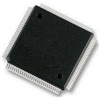
S9S12HZ128J3VAL Freescale Semiconductor, S9S12HZ128J3VAL Datasheet - Page 629

S9S12HZ128J3VAL
Manufacturer Part Number
S9S12HZ128J3VAL
Description
IC MCU FLASH 112-LQFP
Manufacturer
Freescale Semiconductor
Series
HCS12r
Datasheet
1.S9S12HZ128J3VAL.pdf
(692 pages)
Specifications of S9S12HZ128J3VAL
Core Processor
HCS12
Core Size
16-Bit
Speed
25MHz
Connectivity
CAN, EBI/EMI, I²C, SCI, SPI
Peripherals
LCD, Motor control PWM, POR, PWM, WDT
Number Of I /o
91
Program Memory Size
128KB (128K x 8)
Program Memory Type
FLASH
Eeprom Size
2K x 8
Ram Size
6K x 8
Voltage - Supply (vcc/vdd)
2.35 V ~ 2.75 V
Data Converters
A/D 16x10b
Oscillator Type
Internal
Operating Temperature
-40°C ~ 105°C
Package / Case
112-LQFP
Processor Series
S12HY
Core
HCS12X
Data Bus Width
16 bit
Data Ram Size
6 KB
Interface Type
CAN, I2C, SCI, SPI
Maximum Clock Frequency
50 MHz
Number Of Programmable I/os
85
Number Of Timers
1
Operating Supply Voltage
4.5 V to 5.5 V
Maximum Operating Temperature
+ 105 C
Mounting Style
SMD/SMT
Lead Free Status / RoHS Status
Lead free / RoHS Compliant
Available stocks
Company
Part Number
Manufacturer
Quantity
Price
Company:
Part Number:
S9S12HZ128J3VAL
Manufacturer:
Freescale Semiconductor
Quantity:
10 000
Part Number:
S9S12HZ128J3VAL
Manufacturer:
FREESCALE
Quantity:
20 000
Part Number:
S9S12HZ128J3VAL(MC9S12HZ128VAL
Manufacturer:
FREESCALE
Quantity:
20 000
- Current page: 629 of 692
- Download datasheet (4Mb)
2
3
A.1.9
This section describes the characteristics of all 5V I/O pins. All parameters are not always applicable, e.g.
not all pins feature pull up/down resistances.
Freescale Semiconductor
Conditions are shown in
Num C
10
11
12
13
14
PC Board according to EIA/JEDEC Standard 51-2
PC Board according to EIA/JEDEC Standard 51-7
1
2
3
4
5
6
7
8
9
C Input Hysteresis
C Output Rise Time (pins PU and PV in output mode
C Output Fall Time (pins PU and PV in output mode with
P Input High Voltage
P Input Low Voltage
P Input Leakage Current except PU, PV (pins in high
P Input Leakage Current PU, PV (pins in high
P Output High Voltage (pins in output mode, except PU
P Output Low Voltage (pins in output mode except PU
P Output High Voltage (pins PU and PV in output mode)
P Output Low Voltage (pins PU and PV in output mode)
P Internal Pull Up Device Current,
P Internal Pull Up Device Current,
P Internal Pull Down Device Current,
impedance input mode)
V
impedance input mode)
V
and PV)
Partial Drive I OH = –1.0mA
Full Drive I OH = –10mA
and PV)
Partial Drive I OL = +1.0mA
Full Drive I OL = +10mA
I OH = –20mA (typical value at 25 C)
I OL = +20mA (typical value at 25 C)
with slew control enabled) V
to 90% of V
slew control enabled) V
90% of V
tested at V
tested at V
tested at V
in
in
I/O Characteristics
= V
= V
DD5
DD5
OH
IL
IH
IH
or V
or V
OH
Max.
Min.
Min.
Table A-4
SS5
SS5
Rating
DD5
1
2
unless otherwise noted
=5V, R
DD5
=5V, R
MC9S12HZ256 Data Sheet, Rev. 2.05
Table A-6. 5V I/O Characteristics
load
=1K , 10% to
load
=1K , 10%
Symbol
V
I
I
V
V
I
V
V
V
PUH
PDH
V
PUL
HYS
I
I
OH
OH
t
t
OL
OL
in
in
IH
IL
r
f
V
V
0.65*V
V
DD5
DD5
SS5
–1.0
–2.5
Min
–10
60
60
–
–
–
–
– 0.32 V
– 0.3
– 0.8
DD5
Appendix A Electrical Characteristics
DD5
Typ
250
100
100
.2
–
–
–
–
–
–
–
–
–
– 0.2
V
0.35*V
DD5
Max
0.32
–130
130
1.0
2.5
0.8
130
130
–
–
–
+ 0.3
DD5
Unit
mV
ns
ns
V
V
V
V
V
V
A
A
A
A
A
629
Related parts for S9S12HZ128J3VAL
Image
Part Number
Description
Manufacturer
Datasheet
Request
R
Part Number:
Description:
Manufacturer:
Freescale Semiconductor, Inc
Datasheet:
Part Number:
Description:
Manufacturer:
Freescale Semiconductor, Inc
Datasheet:
Part Number:
Description:
Manufacturer:
Freescale Semiconductor, Inc
Datasheet:
Part Number:
Description:
Manufacturer:
Freescale Semiconductor, Inc
Datasheet:
Part Number:
Description:
Manufacturer:
Freescale Semiconductor, Inc
Datasheet:
Part Number:
Description:
Manufacturer:
Freescale Semiconductor, Inc
Datasheet:
Part Number:
Description:
Manufacturer:
Freescale Semiconductor, Inc
Datasheet:
Part Number:
Description:
Manufacturer:
Freescale Semiconductor, Inc
Datasheet:
Part Number:
Description:
Manufacturer:
Freescale Semiconductor, Inc
Datasheet:
Part Number:
Description:
Manufacturer:
Freescale Semiconductor, Inc
Datasheet:
Part Number:
Description:
Manufacturer:
Freescale Semiconductor, Inc
Datasheet:
Part Number:
Description:
Manufacturer:
Freescale Semiconductor, Inc
Datasheet:
Part Number:
Description:
Manufacturer:
Freescale Semiconductor, Inc
Datasheet:
Part Number:
Description:
Manufacturer:
Freescale Semiconductor, Inc
Datasheet:
Part Number:
Description:
Manufacturer:
Freescale Semiconductor, Inc
Datasheet:


