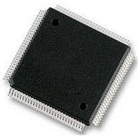
S9S12HZ128J3VAL Freescale Semiconductor, S9S12HZ128J3VAL Datasheet - Page 65

S9S12HZ128J3VAL
Manufacturer Part Number
S9S12HZ128J3VAL
Description
IC MCU FLASH 112-LQFP
Manufacturer
Freescale Semiconductor
Series
HCS12r
Datasheet
1.S9S12HZ128J3VAL.pdf
(692 pages)
Specifications of S9S12HZ128J3VAL
Core Processor
HCS12
Core Size
16-Bit
Speed
25MHz
Connectivity
CAN, EBI/EMI, I²C, SCI, SPI
Peripherals
LCD, Motor control PWM, POR, PWM, WDT
Number Of I /o
91
Program Memory Size
128KB (128K x 8)
Program Memory Type
FLASH
Eeprom Size
2K x 8
Ram Size
6K x 8
Voltage - Supply (vcc/vdd)
2.35 V ~ 2.75 V
Data Converters
A/D 16x10b
Oscillator Type
Internal
Operating Temperature
-40°C ~ 105°C
Package / Case
112-LQFP
Processor Series
S12HY
Core
HCS12X
Data Bus Width
16 bit
Data Ram Size
6 KB
Interface Type
CAN, I2C, SCI, SPI
Maximum Clock Frequency
50 MHz
Number Of Programmable I/os
85
Number Of Timers
1
Operating Supply Voltage
4.5 V to 5.5 V
Maximum Operating Temperature
+ 105 C
Mounting Style
SMD/SMT
Lead Free Status / RoHS Status
Lead free / RoHS Compliant
Available stocks
Company
Part Number
Manufacturer
Quantity
Price
Company:
Part Number:
S9S12HZ128J3VAL
Manufacturer:
Freescale Semiconductor
Quantity:
10 000
Part Number:
S9S12HZ128J3VAL
Manufacturer:
FREESCALE
Quantity:
20 000
Part Number:
S9S12HZ128J3VAL(MC9S12HZ128VAL
Manufacturer:
FREESCALE
Quantity:
20 000
- Current page: 65 of 692
- Download datasheet (4Mb)
2.3.2.1
The unbanked FCLKDIV register is used to control timed events in program and erase algorithms.
All bits in the FCLKDIV register are readable, bits 6-0 are write once and bit 7 is not writable.
2.3.2.2
The unbanked FSEC register holds all bits associated with the security of the MCU and Flash module.
Freescale Semiconductor
FDIV[5:0]
FDIVLD
PRDIV8
RESERVED2
RESERVED3
RESERVED4
Reset
Field
Register
5-0
7
6
Name
W
R
FDIVLD
Clock Divider Loaded.
0 Register has not been written.
1 Register has been written to since the last reset.
Enable Prescalar by 8
0 The oscillator clock is directly fed into the clock divider
1 The oscillator clock is divided by 8 before feeding into the clock divider.
Clock Divider Bits — The combination of PRDIV8 and FDIV[5:0] must divide the oscillator clock down to a
frequency of 150 kHz–200 kHz. The maximum divide ratio is 512. Please refer to
FCLKDIV Register”
Flash Clock Divider Register (FCLKDIV)
Flash Security Register (FSEC)
7
0
W
W
W
R
R
R
= Unimplemented or Reserved
PRDIV8
Bit 7
Figure 2-3. FTS256K2 Register Summary (continued)
0
0
0
6
0
Figure 2-4. Flash Clock Divider Register (FCLKDIV)
for more information.
.
= Unimplemented or Reserved
Table 2-4. FCLKDIV Field Descriptions
6
0
0
0
FDIV5
MC9S12HZ256 Data Sheet, Rev. 2.05
5
0
5
0
0
0
FDIV4
4
0
Description
4
0
0
0
.
FDIV3
3
0
Chapter 2 256 Kbyte Flash Module (FTS256K2V1)
3
0
0
0
FDIV2
2
0
2
0
0
0
Section 2.4.1.1, “Writing the
FDIV1
1
0
1
0
0
0
Bit 0
FDIV0
0
0
0
0
0
65
Related parts for S9S12HZ128J3VAL
Image
Part Number
Description
Manufacturer
Datasheet
Request
R
Part Number:
Description:
Manufacturer:
Freescale Semiconductor, Inc
Datasheet:
Part Number:
Description:
Manufacturer:
Freescale Semiconductor, Inc
Datasheet:
Part Number:
Description:
Manufacturer:
Freescale Semiconductor, Inc
Datasheet:
Part Number:
Description:
Manufacturer:
Freescale Semiconductor, Inc
Datasheet:
Part Number:
Description:
Manufacturer:
Freescale Semiconductor, Inc
Datasheet:
Part Number:
Description:
Manufacturer:
Freescale Semiconductor, Inc
Datasheet:
Part Number:
Description:
Manufacturer:
Freescale Semiconductor, Inc
Datasheet:
Part Number:
Description:
Manufacturer:
Freescale Semiconductor, Inc
Datasheet:
Part Number:
Description:
Manufacturer:
Freescale Semiconductor, Inc
Datasheet:
Part Number:
Description:
Manufacturer:
Freescale Semiconductor, Inc
Datasheet:
Part Number:
Description:
Manufacturer:
Freescale Semiconductor, Inc
Datasheet:
Part Number:
Description:
Manufacturer:
Freescale Semiconductor, Inc
Datasheet:
Part Number:
Description:
Manufacturer:
Freescale Semiconductor, Inc
Datasheet:
Part Number:
Description:
Manufacturer:
Freescale Semiconductor, Inc
Datasheet:
Part Number:
Description:
Manufacturer:
Freescale Semiconductor, Inc
Datasheet:


