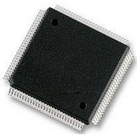
S9S12HZ128J3VAL Freescale Semiconductor, S9S12HZ128J3VAL Datasheet - Page 74

S9S12HZ128J3VAL
Manufacturer Part Number
S9S12HZ128J3VAL
Description
IC MCU FLASH 112-LQFP
Manufacturer
Freescale Semiconductor
Series
HCS12r
Datasheet
1.S9S12HZ128J3VAL.pdf
(692 pages)
Specifications of S9S12HZ128J3VAL
Core Processor
HCS12
Core Size
16-Bit
Speed
25MHz
Connectivity
CAN, EBI/EMI, I²C, SCI, SPI
Peripherals
LCD, Motor control PWM, POR, PWM, WDT
Number Of I /o
91
Program Memory Size
128KB (128K x 8)
Program Memory Type
FLASH
Eeprom Size
2K x 8
Ram Size
6K x 8
Voltage - Supply (vcc/vdd)
2.35 V ~ 2.75 V
Data Converters
A/D 16x10b
Oscillator Type
Internal
Operating Temperature
-40°C ~ 105°C
Package / Case
112-LQFP
Processor Series
S12HY
Core
HCS12X
Data Bus Width
16 bit
Data Ram Size
6 KB
Interface Type
CAN, I2C, SCI, SPI
Maximum Clock Frequency
50 MHz
Number Of Programmable I/os
85
Number Of Timers
1
Operating Supply Voltage
4.5 V to 5.5 V
Maximum Operating Temperature
+ 105 C
Mounting Style
SMD/SMT
Lead Free Status / RoHS Status
Lead free / RoHS Compliant
Available stocks
Company
Part Number
Manufacturer
Quantity
Price
Company:
Part Number:
S9S12HZ128J3VAL
Manufacturer:
Freescale Semiconductor
Quantity:
10 000
Part Number:
S9S12HZ128J3VAL
Manufacturer:
FREESCALE
Quantity:
20 000
Part Number:
S9S12HZ128J3VAL(MC9S12HZ128VAL
Manufacturer:
FREESCALE
Quantity:
20 000
- Current page: 74 of 692
- Download datasheet (4Mb)
Chapter 2 256 Kbyte Flash Module (FTS256K2V1)
All CMDB bits are readable and writable during a command write sequence while bit 7 reads 0 and is not
writable.
2.3.2.9
The banked FCTL register is the Flash control register.
All bits in the FCTL register are readable but are not writable.
The FCTL register is loaded from the Flash Configuration Field byte at $FF0E during the reset sequence,
indicated by F in
74
CMDB[6:0]
NV[7:0]
Reset
Reset
Field
Field
6-0
7-0
W
W
R
R
Flash Command — Valid Flash commands are shown in
listed in
NV7
Nonvolatile Bits — The NV[7:0] bits are available as nonvolatile bits. Refer to the Device User Guide for proper
use of the NV bits.
Flash Control Register (FCTL)
F
7
0
0
7
Figure
Table 2-18
= Unimplemented or Reserved
Figure 2-12. Flash Command Register (FCMD - NVM User Mode)
= Unimplemented or Reserved
2-13.
NV6
6
0
6
F
sets the ACCERR flag in the FSTAT register.
Figure 2-13. Flash Control Register (FCTL)
CMDB[6:0]
Table 2-18. Valid Flash Command List
Table 2-17. FCMD Field Descriptions
Table 2-19. FCTL Field Descriptions
0x05
0x06
0x20
0x40
0x41
0x47
MC9S12HZ256 Data Sheet, Rev. 2.05
NV5
5
0
5
F
NV4
4
0
4
F
Description
Description
Sector Erase Abort
NVM Command
Data Compress
Word Program
Sector Erase
Erase Verify
Mass Erase
CMDB
Table
NV3
F
3
0
3
2-18. Writing any command other than those
NV2
2
0
2
F
Freescale Semiconductor
NV1
1
0
1
F
NV0
F
0
0
0
Related parts for S9S12HZ128J3VAL
Image
Part Number
Description
Manufacturer
Datasheet
Request
R
Part Number:
Description:
Manufacturer:
Freescale Semiconductor, Inc
Datasheet:
Part Number:
Description:
Manufacturer:
Freescale Semiconductor, Inc
Datasheet:
Part Number:
Description:
Manufacturer:
Freescale Semiconductor, Inc
Datasheet:
Part Number:
Description:
Manufacturer:
Freescale Semiconductor, Inc
Datasheet:
Part Number:
Description:
Manufacturer:
Freescale Semiconductor, Inc
Datasheet:
Part Number:
Description:
Manufacturer:
Freescale Semiconductor, Inc
Datasheet:
Part Number:
Description:
Manufacturer:
Freescale Semiconductor, Inc
Datasheet:
Part Number:
Description:
Manufacturer:
Freescale Semiconductor, Inc
Datasheet:
Part Number:
Description:
Manufacturer:
Freescale Semiconductor, Inc
Datasheet:
Part Number:
Description:
Manufacturer:
Freescale Semiconductor, Inc
Datasheet:
Part Number:
Description:
Manufacturer:
Freescale Semiconductor, Inc
Datasheet:
Part Number:
Description:
Manufacturer:
Freescale Semiconductor, Inc
Datasheet:
Part Number:
Description:
Manufacturer:
Freescale Semiconductor, Inc
Datasheet:
Part Number:
Description:
Manufacturer:
Freescale Semiconductor, Inc
Datasheet:
Part Number:
Description:
Manufacturer:
Freescale Semiconductor, Inc
Datasheet:


