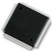
S9S12HZ128J3VAL Freescale Semiconductor, S9S12HZ128J3VAL Datasheet - Page 450

S9S12HZ128J3VAL
Manufacturer Part Number
S9S12HZ128J3VAL
Description
IC MCU FLASH 112-LQFP
Manufacturer
Freescale Semiconductor
Series
HCS12r
Datasheet
1.S9S12HZ128J3VAL.pdf
(692 pages)
Specifications of S9S12HZ128J3VAL
Core Processor
HCS12
Core Size
16-Bit
Speed
25MHz
Connectivity
CAN, EBI/EMI, I²C, SCI, SPI
Peripherals
LCD, Motor control PWM, POR, PWM, WDT
Number Of I /o
91
Program Memory Size
128KB (128K x 8)
Program Memory Type
FLASH
Eeprom Size
2K x 8
Ram Size
6K x 8
Voltage - Supply (vcc/vdd)
2.35 V ~ 2.75 V
Data Converters
A/D 16x10b
Oscillator Type
Internal
Operating Temperature
-40°C ~ 105°C
Package / Case
112-LQFP
Processor Series
S12HY
Core
HCS12X
Data Bus Width
16 bit
Data Ram Size
6 KB
Interface Type
CAN, I2C, SCI, SPI
Maximum Clock Frequency
50 MHz
Number Of Programmable I/os
85
Number Of Timers
1
Operating Supply Voltage
4.5 V to 5.5 V
Maximum Operating Temperature
+ 105 C
Mounting Style
SMD/SMT
Lead Free Status / RoHS Status
Lead free / RoHS Compliant
Available stocks
Company
Part Number
Manufacturer
Quantity
Price
Company:
Part Number:
S9S12HZ128J3VAL
Manufacturer:
Freescale Semiconductor
Quantity:
10 000
Part Number:
S9S12HZ128J3VAL
Manufacturer:
FREESCALE
Quantity:
20 000
Part Number:
S9S12HZ128J3VAL(MC9S12HZ128VAL
Manufacturer:
FREESCALE
Quantity:
20 000
- Current page: 450 of 692
- Download datasheet (4Mb)
Chapter 15 Pulse-Width Modulator (PWM8B6CV1)
15.3.2.4
This register selects the prescale clock source for clocks A and B independently.
Read: anytime
Write: anytime
450
PCKB[2:0]
PCKA[2:0]
PCLK2
PCLK1
PCLK0
Reset
Field
Field
6:5
2:0
2
1
0
W
R
Pulse Width Channel 2 Clock Select
0 Clock B is the clock source for PWM channel 2.
1 Clock SB is the clock source for PWM channel 2.
Pulse Width Channel 1 Clock Select
0 Clock A is the clock source for PWM channel 1.
1 Clock SA is the clock source for PWM channel 1.
Pulse Width Channel 0 Clock Select
0 Clock A is the clock source for PWM channel 0.
1 Clock SA is the clock source for PWM channel 0.
Prescaler Select for Clock B — Clock B is 1 of two clock sources which can be used for channels 2 or 3. These
three bits determine the rate of clock B, as shown in
Prescaler Select for Clock A — Clock A is 1 of two clock sources which can be used for channels 0, 1, 4, or 5.
These three bits determine the rate of clock A, as shown in
PWM Prescale Clock Select Register (PWMPRCLK)
0
0
7
PCKB2–PCKB0 and PCKA2–PCKA0 register bits can be written anytime.
If the clock prescale is changed while a PWM signal is being generated, a
truncated or stretched pulse can occur during the transition.
Figure 15-6. PWM Prescaler Clock Select Register (PWMPRCLK)
= Unimplemented or Reserved
PCKB2
0
6
Table 15-4. PWMCLK Field Descriptions (continued)
Table 15-5. PWMPRCLK Field Descriptions
PCKB1
MC9S12HZ256 Data Sheet, Rev. 2.05
0
5
PCKB0
NOTE
0
4
Description
Description
Table
15-6.
Table
0
0
3
15-7.
PCKA2
0
2
PCKA1
Freescale Semiconductor
0
1
PCKA0
0
0
Related parts for S9S12HZ128J3VAL
Image
Part Number
Description
Manufacturer
Datasheet
Request
R
Part Number:
Description:
Manufacturer:
Freescale Semiconductor, Inc
Datasheet:
Part Number:
Description:
Manufacturer:
Freescale Semiconductor, Inc
Datasheet:
Part Number:
Description:
Manufacturer:
Freescale Semiconductor, Inc
Datasheet:
Part Number:
Description:
Manufacturer:
Freescale Semiconductor, Inc
Datasheet:
Part Number:
Description:
Manufacturer:
Freescale Semiconductor, Inc
Datasheet:
Part Number:
Description:
Manufacturer:
Freescale Semiconductor, Inc
Datasheet:
Part Number:
Description:
Manufacturer:
Freescale Semiconductor, Inc
Datasheet:
Part Number:
Description:
Manufacturer:
Freescale Semiconductor, Inc
Datasheet:
Part Number:
Description:
Manufacturer:
Freescale Semiconductor, Inc
Datasheet:
Part Number:
Description:
Manufacturer:
Freescale Semiconductor, Inc
Datasheet:
Part Number:
Description:
Manufacturer:
Freescale Semiconductor, Inc
Datasheet:
Part Number:
Description:
Manufacturer:
Freescale Semiconductor, Inc
Datasheet:
Part Number:
Description:
Manufacturer:
Freescale Semiconductor, Inc
Datasheet:
Part Number:
Description:
Manufacturer:
Freescale Semiconductor, Inc
Datasheet:
Part Number:
Description:
Manufacturer:
Freescale Semiconductor, Inc
Datasheet:


