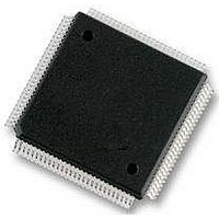
S9S12HZ128J3VAL Freescale Semiconductor, S9S12HZ128J3VAL Datasheet - Page 597

S9S12HZ128J3VAL
Manufacturer Part Number
S9S12HZ128J3VAL
Description
IC MCU FLASH 112-LQFP
Manufacturer
Freescale Semiconductor
Series
HCS12r
Datasheet
1.S9S12HZ128J3VAL.pdf
(692 pages)
Specifications of S9S12HZ128J3VAL
Core Processor
HCS12
Core Size
16-Bit
Speed
25MHz
Connectivity
CAN, EBI/EMI, I²C, SCI, SPI
Peripherals
LCD, Motor control PWM, POR, PWM, WDT
Number Of I /o
91
Program Memory Size
128KB (128K x 8)
Program Memory Type
FLASH
Eeprom Size
2K x 8
Ram Size
6K x 8
Voltage - Supply (vcc/vdd)
2.35 V ~ 2.75 V
Data Converters
A/D 16x10b
Oscillator Type
Internal
Operating Temperature
-40°C ~ 105°C
Package / Case
112-LQFP
Processor Series
S12HY
Core
HCS12X
Data Bus Width
16 bit
Data Ram Size
6 KB
Interface Type
CAN, I2C, SCI, SPI
Maximum Clock Frequency
50 MHz
Number Of Programmable I/os
85
Number Of Timers
1
Operating Supply Voltage
4.5 V to 5.5 V
Maximum Operating Temperature
+ 105 C
Mounting Style
SMD/SMT
Lead Free Status / RoHS Status
Lead free / RoHS Compliant
Available stocks
Company
Part Number
Manufacturer
Quantity
Price
Company:
Part Number:
S9S12HZ128J3VAL
Manufacturer:
Freescale Semiconductor
Quantity:
10 000
Part Number:
S9S12HZ128J3VAL
Manufacturer:
FREESCALE
Quantity:
20 000
Part Number:
S9S12HZ128J3VAL(MC9S12HZ128VAL
Manufacturer:
FREESCALE
Quantity:
20 000
- Current page: 597 of 692
- Download datasheet (4Mb)
21.4.2
In order to allow fast internal bus cycles to coexist in a system with slower external memory resources, the
HCS12 supports the concept of stretched bus cycles (module timing reference clocks for timers and baud
rate generators are not affected by this stretching). Control bits in the MISC register in the MMC sub-block
of the core specify the amount of stretch (0, 1, 2, or 3 periods of the internal bus-rate clock). While
stretching, the CPU state machines are all held in their current state. At this point in the CPU bus cycle,
write data would already be driven onto the data bus so the length of time write data is valid is extended
in the case of a stretched bus cycle. Read data would not be captured by the system until the E clock falling
edge. In the case of a stretched bus cycle, read data is not required until the specified setup time before the
falling edge of the stretched E clock. The chip selects, and R/W signals remain valid during the period of
stretching (throughout the stretched E high time).
21.4.3
The operating mode out of reset is determined by the states of the MODC, MODB, and MODA pins during
reset
operating mode and provide limited mode switching during operation. The states of the MODC, MODB,
and MODA pins are latched into these bits on the rising edge of the reset signal.
Freescale Semiconductor
(Table
MODC
0
0
0
0
1
1
1
1
Stretched Bus Cycles
Modes of Operation
21-16). The MODC, MODB, and MODA bits in the MODE register show the current
The address portion of the bus cycle is not stretched
MODB
LSTRB
0
0
1
1
0
0
1
1
1
0
1
Table 21-15. Access Type vs. Bus Control Pins
MODA
AB0
1
0
1
0
1
0
1
0
1
0
1
MC9S12HZ256 Data Sheet, Rev. 2.05
Table 21-16. Mode Selection
Special Single Chip, BDM allowed and ACTIVE. BDM is allowed in all
other modes but a serial command is required to make BDM active.
Emulation Expanded Narrow, BDM allowed
Special Test (Expanded Wide), BDM allowed
Emulation Expanded Wide, BDM allowed
Normal Single Chip, BDM allowed
Normal Expanded Narrow, BDM allowed
Peripheral; BDM allowed but bus operations would cause bus conflicts
(must not be used)
Normal Expanded Wide, BDM allowed
R/W
1
0
0
NOTE
16-bit read of an odd address
(low/high data swapped)
16-bit write to an even address
16-bit write to an odd address
(low/high data swapped)
Chapter 21 Multiplexed External Bus Interface (MEBIV3)
Mode Description
Type of Access
.
597
Related parts for S9S12HZ128J3VAL
Image
Part Number
Description
Manufacturer
Datasheet
Request
R
Part Number:
Description:
Manufacturer:
Freescale Semiconductor, Inc
Datasheet:
Part Number:
Description:
Manufacturer:
Freescale Semiconductor, Inc
Datasheet:
Part Number:
Description:
Manufacturer:
Freescale Semiconductor, Inc
Datasheet:
Part Number:
Description:
Manufacturer:
Freescale Semiconductor, Inc
Datasheet:
Part Number:
Description:
Manufacturer:
Freescale Semiconductor, Inc
Datasheet:
Part Number:
Description:
Manufacturer:
Freescale Semiconductor, Inc
Datasheet:
Part Number:
Description:
Manufacturer:
Freescale Semiconductor, Inc
Datasheet:
Part Number:
Description:
Manufacturer:
Freescale Semiconductor, Inc
Datasheet:
Part Number:
Description:
Manufacturer:
Freescale Semiconductor, Inc
Datasheet:
Part Number:
Description:
Manufacturer:
Freescale Semiconductor, Inc
Datasheet:
Part Number:
Description:
Manufacturer:
Freescale Semiconductor, Inc
Datasheet:
Part Number:
Description:
Manufacturer:
Freescale Semiconductor, Inc
Datasheet:
Part Number:
Description:
Manufacturer:
Freescale Semiconductor, Inc
Datasheet:
Part Number:
Description:
Manufacturer:
Freescale Semiconductor, Inc
Datasheet:
Part Number:
Description:
Manufacturer:
Freescale Semiconductor, Inc
Datasheet:


