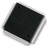
S9S12HZ128J3VAL Freescale Semiconductor, S9S12HZ128J3VAL Datasheet - Page 618

S9S12HZ128J3VAL
Manufacturer Part Number
S9S12HZ128J3VAL
Description
IC MCU FLASH 112-LQFP
Manufacturer
Freescale Semiconductor
Series
HCS12r
Datasheet
1.S9S12HZ128J3VAL.pdf
(692 pages)
Specifications of S9S12HZ128J3VAL
Core Processor
HCS12
Core Size
16-Bit
Speed
25MHz
Connectivity
CAN, EBI/EMI, I²C, SCI, SPI
Peripherals
LCD, Motor control PWM, POR, PWM, WDT
Number Of I /o
91
Program Memory Size
128KB (128K x 8)
Program Memory Type
FLASH
Eeprom Size
2K x 8
Ram Size
6K x 8
Voltage - Supply (vcc/vdd)
2.35 V ~ 2.75 V
Data Converters
A/D 16x10b
Oscillator Type
Internal
Operating Temperature
-40°C ~ 105°C
Package / Case
112-LQFP
Processor Series
S12HY
Core
HCS12X
Data Bus Width
16 bit
Data Ram Size
6 KB
Interface Type
CAN, I2C, SCI, SPI
Maximum Clock Frequency
50 MHz
Number Of Programmable I/os
85
Number Of Timers
1
Operating Supply Voltage
4.5 V to 5.5 V
Maximum Operating Temperature
+ 105 C
Mounting Style
SMD/SMT
Lead Free Status / RoHS Status
Lead free / RoHS Compliant
Available stocks
Company
Part Number
Manufacturer
Quantity
Price
Company:
Part Number:
S9S12HZ128J3VAL
Manufacturer:
Freescale Semiconductor
Quantity:
10 000
Part Number:
S9S12HZ128J3VAL
Manufacturer:
FREESCALE
Quantity:
20 000
Part Number:
S9S12HZ128J3VAL(MC9S12HZ128VAL
Manufacturer:
FREESCALE
Quantity:
20 000
- Current page: 618 of 692
- Download datasheet (4Mb)
Chapter 22 Module Mapping Control (MMCV4)
The PPAGE register holds the page select value for the program page window. The value of the PPAGE
register can be manipulated by normal read and write (some devices don’t allow writes in some modes)
instructions as well as the CALL and RTC instructions.
Control registers, vector spaces, and a portion of on-chip memory are located in unpaged portions of the
64K byte physical address space. The stack and I/O addresses should also be in unpaged memory to make
them accessible from any page.
The starting address of a service routine must be located in unpaged memory because the 16-bit exception
vectors cannot point to addresses in paged memory. However, a service routine can call other routines that
are in paged memory. The upper 16K byte block of memory space (0xC000–0xFFFF) is unpaged. It is
recommended that all reset and interrupt vectors point to locations in this area.
22.4.3.1
CALL and RTC are uninterruptable instructions that automate page switching in the program expansion
window. CALL is similar to a JSR instruction, but the subroutine that is called can be located anywhere in
the normal 64K byte address space or on any page of program expansion memory. CALL calculates and
stacks a return address, stacks the current PPAGE value, and writes a new instruction-supplied value to
PPAGE. The PPAGE value controls which of the 64 possible pages is visible through the 16K byte
expansion window in the 64K byte memory map. Execution then begins at the address of the called
subroutine.
During the execution of a CALL instruction, the CPU:
618
•
Writes the old PPAGE value into an internal temporary register and writes the new
instruction-supplied PPAGE value into the PPAGE register.
CALL and Return from Call Instructions
The partitioning as defined in
memory space and the actual on-chip memory sizes implemented in the
system may differ. Please refer to the device overview chapter for actual
sizes.
pag_sw1:pag_sw0
00
01
10
11
Table 22-17. External/Internal Page Window Access
MC9S12HZ256 Data Sheet, Rev. 2.05
876K off-Chip,
128K on-Chip
768K off-chip,
512K off-chip,
256K on-chip
512K on-chip
Partitioning
0K off-chip,
1M on-chip
Table 22-17
NOTE
0x0038–0x003F
0x0000–0x002F
0x0030–0x003F
0x0000–0x001F
0x0020–0x003F
0x0000–0x003F
0x0000–0x0037
PIX5:0 Value
applies only to the allocated
N/A
Page Window
External
External
External
External
Access
Internal
Internal
Internal
Internal
Freescale Semiconductor
Related parts for S9S12HZ128J3VAL
Image
Part Number
Description
Manufacturer
Datasheet
Request
R
Part Number:
Description:
Manufacturer:
Freescale Semiconductor, Inc
Datasheet:
Part Number:
Description:
Manufacturer:
Freescale Semiconductor, Inc
Datasheet:
Part Number:
Description:
Manufacturer:
Freescale Semiconductor, Inc
Datasheet:
Part Number:
Description:
Manufacturer:
Freescale Semiconductor, Inc
Datasheet:
Part Number:
Description:
Manufacturer:
Freescale Semiconductor, Inc
Datasheet:
Part Number:
Description:
Manufacturer:
Freescale Semiconductor, Inc
Datasheet:
Part Number:
Description:
Manufacturer:
Freescale Semiconductor, Inc
Datasheet:
Part Number:
Description:
Manufacturer:
Freescale Semiconductor, Inc
Datasheet:
Part Number:
Description:
Manufacturer:
Freescale Semiconductor, Inc
Datasheet:
Part Number:
Description:
Manufacturer:
Freescale Semiconductor, Inc
Datasheet:
Part Number:
Description:
Manufacturer:
Freescale Semiconductor, Inc
Datasheet:
Part Number:
Description:
Manufacturer:
Freescale Semiconductor, Inc
Datasheet:
Part Number:
Description:
Manufacturer:
Freescale Semiconductor, Inc
Datasheet:
Part Number:
Description:
Manufacturer:
Freescale Semiconductor, Inc
Datasheet:
Part Number:
Description:
Manufacturer:
Freescale Semiconductor, Inc
Datasheet:


