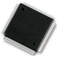
S9S12HZ128J3VAL Freescale Semiconductor, S9S12HZ128J3VAL Datasheet - Page 627

S9S12HZ128J3VAL
Manufacturer Part Number
S9S12HZ128J3VAL
Description
IC MCU FLASH 112-LQFP
Manufacturer
Freescale Semiconductor
Series
HCS12r
Datasheet
1.S9S12HZ128J3VAL.pdf
(692 pages)
Specifications of S9S12HZ128J3VAL
Core Processor
HCS12
Core Size
16-Bit
Speed
25MHz
Connectivity
CAN, EBI/EMI, I²C, SCI, SPI
Peripherals
LCD, Motor control PWM, POR, PWM, WDT
Number Of I /o
91
Program Memory Size
128KB (128K x 8)
Program Memory Type
FLASH
Eeprom Size
2K x 8
Ram Size
6K x 8
Voltage - Supply (vcc/vdd)
2.35 V ~ 2.75 V
Data Converters
A/D 16x10b
Oscillator Type
Internal
Operating Temperature
-40°C ~ 105°C
Package / Case
112-LQFP
Processor Series
S12HY
Core
HCS12X
Data Bus Width
16 bit
Data Ram Size
6 KB
Interface Type
CAN, I2C, SCI, SPI
Maximum Clock Frequency
50 MHz
Number Of Programmable I/os
85
Number Of Timers
1
Operating Supply Voltage
4.5 V to 5.5 V
Maximum Operating Temperature
+ 105 C
Mounting Style
SMD/SMT
Lead Free Status / RoHS Status
Lead free / RoHS Compliant
Available stocks
Company
Part Number
Manufacturer
Quantity
Price
Company:
Part Number:
S9S12HZ128J3VAL
Manufacturer:
Freescale Semiconductor
Quantity:
10 000
Part Number:
S9S12HZ128J3VAL
Manufacturer:
FREESCALE
Quantity:
20 000
Part Number:
S9S12HZ128J3VAL(MC9S12HZ128VAL
Manufacturer:
FREESCALE
Quantity:
20 000
- Current page: 627 of 692
- Download datasheet (4Mb)
A.1.7
This chapter describes the operating conditions of the device. Unless otherwise noted those conditions
apply to all the following data.
Freescale Semiconductor
1
2
I/O, Regulator and Analog Supply Voltage
Digital Logic Supply Voltage
PLL Supply Voltage
Voltage Difference VDDX to VDDR and VDDA
Voltage Difference VSSX to VSSR and VSSA
Crystal oscillator (Colpitts)
Crystal oscillator (Pierce)
Bus Frequency
Operating Junction Temperature Range
Operating Ambient Temperature Range
The device contains an internal voltage regulator to generate the logic and PLL supply out of the I/O supply. The
absolute maximum ratings apply when this regulator is disabled and the device is powered from an external source.
Please refer to
between ambient temperature T
4
5
C Latch-up Current at T
C Latch-up Current at T
Operating Conditions
positive
negative
positive
negative
Please refer to the temperature rating of the device (C, V, M) with regards to
the ambient temperature T
dissipation calculations refer to
Thermal
Section A.1.8, “Power Dissipation and Thermal
2
Rating
Characteristics.”
Table A-3. ESD and Latch-Up Protection Characteristics
1
A
A
A
and device junction temperature T
= 125 C
= 27 C
MC9S12HZ256 Data Sheet, Rev. 2.05
Table A-4. Operating Conditions
2
A
M parts
M parts
C parts
C parts
V parts
V parts
and the junction temperature T
Section A.1.8, “Power Dissipation and
NOTE
Symbol
V
V
DDPLL
V
VDDX
VSSX
f
f
f
osc
osc
bus
T
T
DD5
DD
A
J
Characteristics,” for more details about the relation
J
.
I
I
LAT
LAT
2.35
2.35
–0.1
–0.1
Min
–40
–40
4.5
0.5
0.5
0.5
+100
–100
+200
–200
J
. For power
Appendix A Electrical Characteristics
Typ
2.5
2.5
27
5
0
0
–
–
–
–
–
–
Max
2.75
2.75
100
120
140
105
125
5.5
0.1
0.1
16
40
25
85
mA
mA
MHz
MHz
MHz
Unit
V
V
V
V
V
C
C
627
Related parts for S9S12HZ128J3VAL
Image
Part Number
Description
Manufacturer
Datasheet
Request
R
Part Number:
Description:
Manufacturer:
Freescale Semiconductor, Inc
Datasheet:
Part Number:
Description:
Manufacturer:
Freescale Semiconductor, Inc
Datasheet:
Part Number:
Description:
Manufacturer:
Freescale Semiconductor, Inc
Datasheet:
Part Number:
Description:
Manufacturer:
Freescale Semiconductor, Inc
Datasheet:
Part Number:
Description:
Manufacturer:
Freescale Semiconductor, Inc
Datasheet:
Part Number:
Description:
Manufacturer:
Freescale Semiconductor, Inc
Datasheet:
Part Number:
Description:
Manufacturer:
Freescale Semiconductor, Inc
Datasheet:
Part Number:
Description:
Manufacturer:
Freescale Semiconductor, Inc
Datasheet:
Part Number:
Description:
Manufacturer:
Freescale Semiconductor, Inc
Datasheet:
Part Number:
Description:
Manufacturer:
Freescale Semiconductor, Inc
Datasheet:
Part Number:
Description:
Manufacturer:
Freescale Semiconductor, Inc
Datasheet:
Part Number:
Description:
Manufacturer:
Freescale Semiconductor, Inc
Datasheet:
Part Number:
Description:
Manufacturer:
Freescale Semiconductor, Inc
Datasheet:
Part Number:
Description:
Manufacturer:
Freescale Semiconductor, Inc
Datasheet:
Part Number:
Description:
Manufacturer:
Freescale Semiconductor, Inc
Datasheet:


