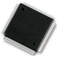
S9S12HZ128J3VAL Freescale Semiconductor, S9S12HZ128J3VAL Datasheet - Page 537

S9S12HZ128J3VAL
Manufacturer Part Number
S9S12HZ128J3VAL
Description
IC MCU FLASH 112-LQFP
Manufacturer
Freescale Semiconductor
Series
HCS12r
Datasheet
1.S9S12HZ128J3VAL.pdf
(692 pages)
Specifications of S9S12HZ128J3VAL
Core Processor
HCS12
Core Size
16-Bit
Speed
25MHz
Connectivity
CAN, EBI/EMI, I²C, SCI, SPI
Peripherals
LCD, Motor control PWM, POR, PWM, WDT
Number Of I /o
91
Program Memory Size
128KB (128K x 8)
Program Memory Type
FLASH
Eeprom Size
2K x 8
Ram Size
6K x 8
Voltage - Supply (vcc/vdd)
2.35 V ~ 2.75 V
Data Converters
A/D 16x10b
Oscillator Type
Internal
Operating Temperature
-40°C ~ 105°C
Package / Case
112-LQFP
Processor Series
S12HY
Core
HCS12X
Data Bus Width
16 bit
Data Ram Size
6 KB
Interface Type
CAN, I2C, SCI, SPI
Maximum Clock Frequency
50 MHz
Number Of Programmable I/os
85
Number Of Timers
1
Operating Supply Voltage
4.5 V to 5.5 V
Maximum Operating Temperature
+ 105 C
Mounting Style
SMD/SMT
Lead Free Status / RoHS Status
Lead free / RoHS Compliant
Available stocks
Company
Part Number
Manufacturer
Quantity
Price
Company:
Part Number:
S9S12HZ128J3VAL
Manufacturer:
Freescale Semiconductor
Quantity:
10 000
Part Number:
S9S12HZ128J3VAL
Manufacturer:
FREESCALE
Quantity:
20 000
Part Number:
S9S12HZ128J3VAL(MC9S12HZ128VAL
Manufacturer:
FREESCALE
Quantity:
20 000
- Current page: 537 of 692
- Download datasheet (4Mb)
19.1.2
There are two main modes of operation: breakpoint mode and debug mode. Each one is mutually exclusive
of the other and selected via a software programmable control bit.
In the breakpoint mode there are two sub-modes of operation:
In debug mode, there are several sub-modes of operation.
19.1.3
Figure 19-1
module in debug mode.
Freescale Semiconductor
•
•
•
•
— Data associated with event B trigger modes
— Detail report mode stores address and data for all cycles except program (P) and free (f) cycles
— Current instruction address when in profiling mode
— BGND is not considered a change-of-flow (cof) by the debugger
Dual address mode, where a match on either of two addresses will cause the system to enter
background debug mode (BDM) or initiate a software interrupt (SWI).
Full breakpoint mode, where a match on address and data will cause the system to enter
background debug mode (BDM) or initiate a software interrupt (SWI).
Trigger modes
There are many ways to create a logical trigger. The trigger can be used to capture bus information
either starting from the trigger or ending at the trigger. Types of triggers (A and B are registers):
— A only
— A or B
— A then B
— Event only B (data capture)
— A then event only B (data capture)
— A and B, full mode
— A and not B, full mode
— Inside range
— Outside range
Capture modes
There are several capture modes. These determine which bus information is saved and which is
ignored.
— Normal: save change-of-flow program fetches
— Loop1: save change-of-flow program fetches, ignoring duplicates
— Detail: save all bus operations except program and free cycles
— Profile: poll target from external device
Modes of Operation
Block Diagram
is a block diagram of this module in breakpoint mode.
MC9S12HZ256 Data Sheet, Rev. 2.05
Figure 19-2
Chapter 19 Debug Module (DBGV1)
is a block diagram of this
537
Related parts for S9S12HZ128J3VAL
Image
Part Number
Description
Manufacturer
Datasheet
Request
R
Part Number:
Description:
Manufacturer:
Freescale Semiconductor, Inc
Datasheet:
Part Number:
Description:
Manufacturer:
Freescale Semiconductor, Inc
Datasheet:
Part Number:
Description:
Manufacturer:
Freescale Semiconductor, Inc
Datasheet:
Part Number:
Description:
Manufacturer:
Freescale Semiconductor, Inc
Datasheet:
Part Number:
Description:
Manufacturer:
Freescale Semiconductor, Inc
Datasheet:
Part Number:
Description:
Manufacturer:
Freescale Semiconductor, Inc
Datasheet:
Part Number:
Description:
Manufacturer:
Freescale Semiconductor, Inc
Datasheet:
Part Number:
Description:
Manufacturer:
Freescale Semiconductor, Inc
Datasheet:
Part Number:
Description:
Manufacturer:
Freescale Semiconductor, Inc
Datasheet:
Part Number:
Description:
Manufacturer:
Freescale Semiconductor, Inc
Datasheet:
Part Number:
Description:
Manufacturer:
Freescale Semiconductor, Inc
Datasheet:
Part Number:
Description:
Manufacturer:
Freescale Semiconductor, Inc
Datasheet:
Part Number:
Description:
Manufacturer:
Freescale Semiconductor, Inc
Datasheet:
Part Number:
Description:
Manufacturer:
Freescale Semiconductor, Inc
Datasheet:
Part Number:
Description:
Manufacturer:
Freescale Semiconductor, Inc
Datasheet:


