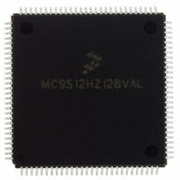
MC9S12HZ128VAL Freescale Semiconductor, MC9S12HZ128VAL Datasheet - Page 156

MC9S12HZ128VAL
Manufacturer Part Number
MC9S12HZ128VAL
Description
IC MCU 16BIT 2K FLASH 112-LQFP
Manufacturer
Freescale Semiconductor
Series
HCS12r
Datasheet
1.MC9S12HZ128CAL.pdf
(692 pages)
Specifications of MC9S12HZ128VAL
Core Processor
HCS12
Core Size
16-Bit
Speed
25MHz
Connectivity
CAN, EBI/EMI, I²C, SCI, SPI
Peripherals
LCD, Motor control PWM, POR, PWM, WDT
Number Of I /o
85
Program Memory Size
128KB (128K x 8)
Program Memory Type
FLASH
Eeprom Size
2K x 8
Ram Size
6K x 8
Voltage - Supply (vcc/vdd)
2.35 V ~ 5.5 V
Data Converters
A/D 16x10b
Oscillator Type
Internal
Operating Temperature
-40°C ~ 105°C
Package / Case
112-LQFP
Processor Series
S12H
Core
HCS12
Data Bus Width
16 bit
Data Ram Size
6 KB
Interface Type
I2C/SCI/SPI
Maximum Clock Frequency
50 MHz
Number Of Programmable I/os
85
Number Of Timers
8
Maximum Operating Temperature
+ 105 C
Mounting Style
SMD/SMT
3rd Party Development Tools
EWHCS12
Minimum Operating Temperature
- 40 C
On-chip Adc
16-ch x 10-bit
Lead Free Status / RoHS Status
Lead free / RoHS Compliant
Available stocks
Company
Part Number
Manufacturer
Quantity
Price
Company:
Part Number:
MC9S12HZ128VAL
Manufacturer:
Freescale Semiconductor
Quantity:
10 000
Part Number:
MC9S12HZ128VAL
Manufacturer:
FREESCALE
Quantity:
20 000
- Current page: 156 of 692
- Download datasheet (4Mb)
Chapter 4 Port Integration Module (PIM9HZ256V2)
4.3.8
Port V is associated with the stepper stall detect (SSD3 and SSD2) and motor controller (MC3 and MC2)
modules. Each pin is assigned to these modules according to the following priority: SSD3/SSD2 >
MC3/MC2 > general-purpose I/O.
If SSD3 module is enabled, the PV[7:4] pins are controlled by the SSD3 module. If SSD3 module is
disabled, the PV[7:4] pins are controlled by the motor control PWM channels 7 and 6 (MC3).
If SSD2 module is enabled, the PV[3:0] pins are controlled by the SSD2 module. If SSD2 module is
disabled, the PV[3:0] pins are controlled by the motor control PWM channels 5 and 4 (MC2).
Refer to the SSD and MC block description chapters for information on enabling and disabling the SSD
module and the motor control PWM channels respectively.
During reset, port V pins are configured as high-impedance inputs.
4.3.8.1
Read: Anytime. Write: anytime.
If the associated data direction bit (DDRVx) is set to 1 (output), a read returns the value of the I/O register
bit.
If the associated data direction bit (DDRVx) is set to 0 (input) and the slew rate is enabled, the associated
I/O register bit (PTVx) reads “1”.
If the associated data direction bit (DDRVx) is set to 0 (input) and the slew rate is disabled, a read returns
the value of the pin.
156
SSD3/
SSD2
Reset
MC:
W
R
M3SINP
M3C1P
Port V
PTV7
Port V I/O Register (PTV)
0
7
M3SINM
M3C1M
PTV6
0
6
Figure 4-49. Port V I/O Register (PTV)
M3COSP
M3C0P
PTV5
MC9S12HZ256 Data Sheet, Rev. 2.05
0
5
M3COSM
M3C0M
PTV4
0
4
M2SINP
M2C1P
PTV3
0
3
M2SINM
M2C1M
PTV2
0
2
M2COSP
M2C0P
Freescale Semiconductor
PTV1
0
1
M2COSM
M2C0M
PTV0
0
0
Related parts for MC9S12HZ128VAL
Image
Part Number
Description
Manufacturer
Datasheet
Request
R
Part Number:
Description:
Manufacturer:
Freescale Semiconductor, Inc
Datasheet:
Part Number:
Description:
Manufacturer:
Freescale Semiconductor, Inc
Datasheet:
Part Number:
Description:
Manufacturer:
Freescale Semiconductor, Inc
Datasheet:
Part Number:
Description:
Manufacturer:
Freescale Semiconductor, Inc
Datasheet:
Part Number:
Description:
Manufacturer:
Freescale Semiconductor, Inc
Datasheet:
Part Number:
Description:
Manufacturer:
Freescale Semiconductor, Inc
Datasheet:
Part Number:
Description:
Manufacturer:
Freescale Semiconductor, Inc
Datasheet:
Part Number:
Description:
Manufacturer:
Freescale Semiconductor, Inc
Datasheet:
Part Number:
Description:
Manufacturer:
Freescale Semiconductor, Inc
Datasheet:
Part Number:
Description:
Manufacturer:
Freescale Semiconductor, Inc
Datasheet:
Part Number:
Description:
Manufacturer:
Freescale Semiconductor, Inc
Datasheet:
Part Number:
Description:
Manufacturer:
Freescale Semiconductor, Inc
Datasheet:
Part Number:
Description:
Manufacturer:
Freescale Semiconductor, Inc
Datasheet:
Part Number:
Description:
Manufacturer:
Freescale Semiconductor, Inc
Datasheet:
Part Number:
Description:
Manufacturer:
Freescale Semiconductor, Inc
Datasheet:


