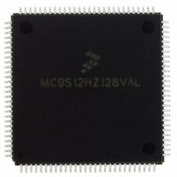
MC9S12HZ128VAL Freescale Semiconductor, MC9S12HZ128VAL Datasheet - Page 497

MC9S12HZ128VAL
Manufacturer Part Number
MC9S12HZ128VAL
Description
IC MCU 16BIT 2K FLASH 112-LQFP
Manufacturer
Freescale Semiconductor
Series
HCS12r
Datasheet
1.MC9S12HZ128CAL.pdf
(692 pages)
Specifications of MC9S12HZ128VAL
Core Processor
HCS12
Core Size
16-Bit
Speed
25MHz
Connectivity
CAN, EBI/EMI, I²C, SCI, SPI
Peripherals
LCD, Motor control PWM, POR, PWM, WDT
Number Of I /o
85
Program Memory Size
128KB (128K x 8)
Program Memory Type
FLASH
Eeprom Size
2K x 8
Ram Size
6K x 8
Voltage - Supply (vcc/vdd)
2.35 V ~ 5.5 V
Data Converters
A/D 16x10b
Oscillator Type
Internal
Operating Temperature
-40°C ~ 105°C
Package / Case
112-LQFP
Processor Series
S12H
Core
HCS12
Data Bus Width
16 bit
Data Ram Size
6 KB
Interface Type
I2C/SCI/SPI
Maximum Clock Frequency
50 MHz
Number Of Programmable I/os
85
Number Of Timers
8
Maximum Operating Temperature
+ 105 C
Mounting Style
SMD/SMT
3rd Party Development Tools
EWHCS12
Minimum Operating Temperature
- 40 C
On-chip Adc
16-ch x 10-bit
Lead Free Status / RoHS Status
Lead free / RoHS Compliant
Available stocks
Company
Part Number
Manufacturer
Quantity
Price
Company:
Part Number:
MC9S12HZ128VAL
Manufacturer:
Freescale Semiconductor
Quantity:
10 000
Part Number:
MC9S12HZ128VAL
Manufacturer:
FREESCALE
Quantity:
20 000
- Current page: 497 of 692
- Download datasheet (4Mb)
16.4.2
Clearing the I/O (input/output) select bit, IOSx, configures channel x as an input capture channel. The
input capture function captures the time at which an external event occurs. When an active edge occurs on
the pin of an input capture channel, the timer transfers the value in the timer counter into the timer channel
registers, TCx.
The minimum pulse width for the input capture input is greater than two bus clocks.
An input capture on channel x sets the CxF flag. The CxI bit enables the CxF flag to generate interrupt
requests.
16.4.3
Setting the I/O select bit, IOSx, configures channel x as an output compare channel. The output compare
function can generate a periodic pulse with a programmable polarity, duration, and frequency. When the
timer counter reaches the value in the channel registers of an output compare channel, the timer can set,
clear, or toggle the channel pin. An output compare on channel x sets the CxF flag. The CxI bit enables the
CxF flag to generate interrupt requests.
The output mode and level bits, OMx and OLx, select set, clear, toggle on output compare. Clearing both
OMx and OLx disconnects the pin from the output logic.
Setting a force output compare bit, FOCx, causes an output compare on channel x. A forced output
compare does not set the channel flag.
A successful output compare on channel 7 overrides output compares on all other output compare
channels. The output compare 7 mask register masks the bits in the output compare 7 data register. The
timer counter reset enable bit, TCRE, enables channel 7 output compares to reset the timer counter. A
channel 7 output compare can reset the timer counter even if the IOC7 pin is being used as the pulse
accumulator input.
Writing to the timer port bit of an output compare pin does not affect the pin state. The value written is
stored in an internal latch. When the pin becomes available for general-purpose output, the last value
written to the bit appears at the pin.
16.4.4
The pulse accumulator (PACNT) is a 16-bit counter that can operate in two modes:
Event counter mode — Counting edges of selected polarity on the pulse accumulator input pin, PAI.
Gated time accumulation mode — Counting pulses from a divide-by-64 clock. The PAMOD bit selects the
mode of operation.
The minimum pulse width for the PAI input is greater than two bus clocks.
Freescale Semiconductor
Input Capture
Output Compare
Pulse Accumulator
MC9S12HZ256 Data Sheet, Rev. 2.05
Chapter 16 Timer Module (TIM16B8CV1)
497
Related parts for MC9S12HZ128VAL
Image
Part Number
Description
Manufacturer
Datasheet
Request
R
Part Number:
Description:
Manufacturer:
Freescale Semiconductor, Inc
Datasheet:
Part Number:
Description:
Manufacturer:
Freescale Semiconductor, Inc
Datasheet:
Part Number:
Description:
Manufacturer:
Freescale Semiconductor, Inc
Datasheet:
Part Number:
Description:
Manufacturer:
Freescale Semiconductor, Inc
Datasheet:
Part Number:
Description:
Manufacturer:
Freescale Semiconductor, Inc
Datasheet:
Part Number:
Description:
Manufacturer:
Freescale Semiconductor, Inc
Datasheet:
Part Number:
Description:
Manufacturer:
Freescale Semiconductor, Inc
Datasheet:
Part Number:
Description:
Manufacturer:
Freescale Semiconductor, Inc
Datasheet:
Part Number:
Description:
Manufacturer:
Freescale Semiconductor, Inc
Datasheet:
Part Number:
Description:
Manufacturer:
Freescale Semiconductor, Inc
Datasheet:
Part Number:
Description:
Manufacturer:
Freescale Semiconductor, Inc
Datasheet:
Part Number:
Description:
Manufacturer:
Freescale Semiconductor, Inc
Datasheet:
Part Number:
Description:
Manufacturer:
Freescale Semiconductor, Inc
Datasheet:
Part Number:
Description:
Manufacturer:
Freescale Semiconductor, Inc
Datasheet:
Part Number:
Description:
Manufacturer:
Freescale Semiconductor, Inc
Datasheet:


