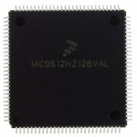
MC9S12HZ128VAL Freescale Semiconductor, MC9S12HZ128VAL Datasheet - Page 44

MC9S12HZ128VAL
Manufacturer Part Number
MC9S12HZ128VAL
Description
IC MCU 16BIT 2K FLASH 112-LQFP
Manufacturer
Freescale Semiconductor
Series
HCS12r
Datasheet
1.MC9S12HZ128CAL.pdf
(692 pages)
Specifications of MC9S12HZ128VAL
Core Processor
HCS12
Core Size
16-Bit
Speed
25MHz
Connectivity
CAN, EBI/EMI, I²C, SCI, SPI
Peripherals
LCD, Motor control PWM, POR, PWM, WDT
Number Of I /o
85
Program Memory Size
128KB (128K x 8)
Program Memory Type
FLASH
Eeprom Size
2K x 8
Ram Size
6K x 8
Voltage - Supply (vcc/vdd)
2.35 V ~ 5.5 V
Data Converters
A/D 16x10b
Oscillator Type
Internal
Operating Temperature
-40°C ~ 105°C
Package / Case
112-LQFP
Processor Series
S12H
Core
HCS12
Data Bus Width
16 bit
Data Ram Size
6 KB
Interface Type
I2C/SCI/SPI
Maximum Clock Frequency
50 MHz
Number Of Programmable I/os
85
Number Of Timers
8
Maximum Operating Temperature
+ 105 C
Mounting Style
SMD/SMT
3rd Party Development Tools
EWHCS12
Minimum Operating Temperature
- 40 C
On-chip Adc
16-ch x 10-bit
Lead Free Status / RoHS Status
Lead free / RoHS Compliant
Available stocks
Company
Part Number
Manufacturer
Quantity
Price
Company:
Part Number:
MC9S12HZ128VAL
Manufacturer:
Freescale Semiconductor
Quantity:
10 000
Part Number:
MC9S12HZ128VAL
Manufacturer:
FREESCALE
Quantity:
20 000
- Current page: 44 of 692
- Download datasheet (4Mb)
Chapter 1 MC9S12HZ256 Device Overview
1.5.6.36
PV7–PV4 are general-purpose input or output pins. They can be configured as high current PWM output
pins which can be used for motor drive or to measure the back EMF to calibrate the pointer reset position.
These pins interface to the coils of motor 3.
1.5.6.37
PV3–PV0 are general-purpose input or output pins. They can be configured as high current PWM output
pins which can be used for motor drive or to measure the back EMF to calibrate the pointer reset position.
These pins interface to the coils of motor 2.
1.5.7
MC9S12HZ256 power and ground pins are described below.
1.5.7.1
V
1.5.7.2
V
and V
1.5.7.3
V
output. These pins serve as connection points for filter capacitors. V
1.5.7.4
V
converter.
44
DDR
DDX1
DD1
DDA
, V
DDX2
, V
is the power supply pin for the internal voltage regulator.
, V
SS1
SSA
DDX2
as well as V
Power Supply Pins
and V
PV[7:4] / M3C1(SIN)P, M3C1(SIN)M, M3C0(COS)P, M3C0(COS)M — Port V
I/O Pins [7:4]
PV[3:0] / M2C1(SIN)P, M2C1(SIN)M, M2C0(COS)P, M2C0(COS)M — Port V
I/O Pins [3:0]
V
V
V
V
are the power supply and ground pins for the voltage regulator and the analog-to-digital
All V
Appendix B, “PCB Layout
Because fast signal transitions place high, short-duration current demands
on the power supply, use bypass capacitors with high-frequency
characteristics and place them as close to the MCU as possible. Bypass
requirements depend on how heavily the MCU pins are loaded
No load allowed except for bypass capacitors.
DDR
DDX1
DD1
DDA
, V
SSX1
SS2
, V
, V
SS
— External Power Pin
, V
are the internal logic power and ground pins and related to the voltage regulator
SS1
SSA
pins must be connected together in the application (See
and V
SSX1
DDX2
, V
— Power Supply Pins for ATD and VREG
and V
SSX2
, V
SS2
SSX1
are the power supply and ground pins for input/output drivers.V
— Internal Logic Power Pins
SSX2
MC9S12HZ256 Data Sheet, Rev. 2.05
, V
are not internally connected.
SSX2
Guidelines”).
— External Power and Ground Pins
NOTE
NOTE
SS1
and V
SS2
(Table
are internally connected.
Freescale Semiconductor
B-1).
DDX1
Related parts for MC9S12HZ128VAL
Image
Part Number
Description
Manufacturer
Datasheet
Request
R
Part Number:
Description:
Manufacturer:
Freescale Semiconductor, Inc
Datasheet:
Part Number:
Description:
Manufacturer:
Freescale Semiconductor, Inc
Datasheet:
Part Number:
Description:
Manufacturer:
Freescale Semiconductor, Inc
Datasheet:
Part Number:
Description:
Manufacturer:
Freescale Semiconductor, Inc
Datasheet:
Part Number:
Description:
Manufacturer:
Freescale Semiconductor, Inc
Datasheet:
Part Number:
Description:
Manufacturer:
Freescale Semiconductor, Inc
Datasheet:
Part Number:
Description:
Manufacturer:
Freescale Semiconductor, Inc
Datasheet:
Part Number:
Description:
Manufacturer:
Freescale Semiconductor, Inc
Datasheet:
Part Number:
Description:
Manufacturer:
Freescale Semiconductor, Inc
Datasheet:
Part Number:
Description:
Manufacturer:
Freescale Semiconductor, Inc
Datasheet:
Part Number:
Description:
Manufacturer:
Freescale Semiconductor, Inc
Datasheet:
Part Number:
Description:
Manufacturer:
Freescale Semiconductor, Inc
Datasheet:
Part Number:
Description:
Manufacturer:
Freescale Semiconductor, Inc
Datasheet:
Part Number:
Description:
Manufacturer:
Freescale Semiconductor, Inc
Datasheet:
Part Number:
Description:
Manufacturer:
Freescale Semiconductor, Inc
Datasheet:


