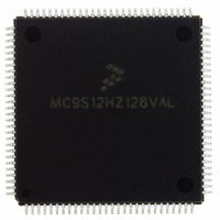
MC9S12HZ128VAL Freescale Semiconductor, MC9S12HZ128VAL Datasheet - Page 335

MC9S12HZ128VAL
Manufacturer Part Number
MC9S12HZ128VAL
Description
IC MCU 16BIT 2K FLASH 112-LQFP
Manufacturer
Freescale Semiconductor
Series
HCS12r
Datasheet
1.MC9S12HZ128CAL.pdf
(692 pages)
Specifications of MC9S12HZ128VAL
Core Processor
HCS12
Core Size
16-Bit
Speed
25MHz
Connectivity
CAN, EBI/EMI, I²C, SCI, SPI
Peripherals
LCD, Motor control PWM, POR, PWM, WDT
Number Of I /o
85
Program Memory Size
128KB (128K x 8)
Program Memory Type
FLASH
Eeprom Size
2K x 8
Ram Size
6K x 8
Voltage - Supply (vcc/vdd)
2.35 V ~ 5.5 V
Data Converters
A/D 16x10b
Oscillator Type
Internal
Operating Temperature
-40°C ~ 105°C
Package / Case
112-LQFP
Processor Series
S12H
Core
HCS12
Data Bus Width
16 bit
Data Ram Size
6 KB
Interface Type
I2C/SCI/SPI
Maximum Clock Frequency
50 MHz
Number Of Programmable I/os
85
Number Of Timers
8
Maximum Operating Temperature
+ 105 C
Mounting Style
SMD/SMT
3rd Party Development Tools
EWHCS12
Minimum Operating Temperature
- 40 C
On-chip Adc
16-ch x 10-bit
Lead Free Status / RoHS Status
Lead free / RoHS Compliant
Available stocks
Company
Part Number
Manufacturer
Quantity
Price
Company:
Part Number:
MC9S12HZ128VAL
Manufacturer:
Freescale Semiconductor
Quantity:
10 000
Part Number:
MC9S12HZ128VAL
Manufacturer:
FREESCALE
Quantity:
20 000
- Current page: 335 of 692
- Download datasheet (4Mb)
12.2.2
TXCAN is the MSCAN transmitter output pin. The TXCAN output pin represents the logic level on the
CAN bus:
12.2.3
A typical CAN system with MSCAN is shown in
to the CAN bus lines through a transceiver device. The transceiver is capable of driving the large current
needed for the CAN bus and has current protection against defective CAN or defective stations.
12.3
This section provides a detailed description of all registers accessible in the MSCAN.
12.3.1
Table 12-1
register address results from the addition of base address and address offset. The base address is
determined at the MCU level and can be found in the
is defined at the module level.
The MSCAN occupies 64 bytes in the memory space. The base address of the MSCAN module is
determined at the MCU level when the MCU is defined. The register decode map is fixed and begins at the
first address of the module address offset.
Table 12-1
base address. The detailed register descriptions follow in the order they appear in the register map.
Freescale Semiconductor
Memory Map and Register Definition
0 = Dominant state
1 = Recessive state
gives an overview on all registers and their individual bits in the MSCAN memory map. The
shows the individual registers associated with the MSCAN and their relative offset from the
TXCAN — CAN Transmitter Output Pin
CAN System
Module Memory Map
TXCAN
CAN_H
CAN node 1
CAN Controller
Transceiver
(MSCAN)
MCU
MC9S12HZ256 Data Sheet, Rev. 2.05
CAN_L
RXCAN
Figure 12-2. CAN System
CAN Bus
Figure
Chapter 12 Freescale’s Scalable Controller Area Network (MSCANV2)
Memory
CAN node 2
12-2. Each CAN station is connected physically
block description chapter. The address offset
CAN node n
335
Related parts for MC9S12HZ128VAL
Image
Part Number
Description
Manufacturer
Datasheet
Request
R
Part Number:
Description:
Manufacturer:
Freescale Semiconductor, Inc
Datasheet:
Part Number:
Description:
Manufacturer:
Freescale Semiconductor, Inc
Datasheet:
Part Number:
Description:
Manufacturer:
Freescale Semiconductor, Inc
Datasheet:
Part Number:
Description:
Manufacturer:
Freescale Semiconductor, Inc
Datasheet:
Part Number:
Description:
Manufacturer:
Freescale Semiconductor, Inc
Datasheet:
Part Number:
Description:
Manufacturer:
Freescale Semiconductor, Inc
Datasheet:
Part Number:
Description:
Manufacturer:
Freescale Semiconductor, Inc
Datasheet:
Part Number:
Description:
Manufacturer:
Freescale Semiconductor, Inc
Datasheet:
Part Number:
Description:
Manufacturer:
Freescale Semiconductor, Inc
Datasheet:
Part Number:
Description:
Manufacturer:
Freescale Semiconductor, Inc
Datasheet:
Part Number:
Description:
Manufacturer:
Freescale Semiconductor, Inc
Datasheet:
Part Number:
Description:
Manufacturer:
Freescale Semiconductor, Inc
Datasheet:
Part Number:
Description:
Manufacturer:
Freescale Semiconductor, Inc
Datasheet:
Part Number:
Description:
Manufacturer:
Freescale Semiconductor, Inc
Datasheet:
Part Number:
Description:
Manufacturer:
Freescale Semiconductor, Inc
Datasheet:


