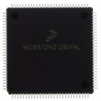
MC9S12HZ128VAL Freescale Semiconductor, MC9S12HZ128VAL Datasheet - Page 596

MC9S12HZ128VAL
Manufacturer Part Number
MC9S12HZ128VAL
Description
IC MCU 16BIT 2K FLASH 112-LQFP
Manufacturer
Freescale Semiconductor
Series
HCS12r
Datasheet
1.MC9S12HZ128CAL.pdf
(692 pages)
Specifications of MC9S12HZ128VAL
Core Processor
HCS12
Core Size
16-Bit
Speed
25MHz
Connectivity
CAN, EBI/EMI, I²C, SCI, SPI
Peripherals
LCD, Motor control PWM, POR, PWM, WDT
Number Of I /o
85
Program Memory Size
128KB (128K x 8)
Program Memory Type
FLASH
Eeprom Size
2K x 8
Ram Size
6K x 8
Voltage - Supply (vcc/vdd)
2.35 V ~ 5.5 V
Data Converters
A/D 16x10b
Oscillator Type
Internal
Operating Temperature
-40°C ~ 105°C
Package / Case
112-LQFP
Processor Series
S12H
Core
HCS12
Data Bus Width
16 bit
Data Ram Size
6 KB
Interface Type
I2C/SCI/SPI
Maximum Clock Frequency
50 MHz
Number Of Programmable I/os
85
Number Of Timers
8
Maximum Operating Temperature
+ 105 C
Mounting Style
SMD/SMT
3rd Party Development Tools
EWHCS12
Minimum Operating Temperature
- 40 C
On-chip Adc
16-ch x 10-bit
Lead Free Status / RoHS Status
Lead free / RoHS Compliant
Available stocks
Company
Part Number
Manufacturer
Quantity
Price
Company:
Part Number:
MC9S12HZ128VAL
Manufacturer:
Freescale Semiconductor
Quantity:
10 000
Part Number:
MC9S12HZ128VAL
Manufacturer:
FREESCALE
Quantity:
20 000
- Current page: 596 of 692
- Download datasheet (4Mb)
Chapter 21 Multiplexed External Bus Interface (MEBIV3)
21.3.2.16 Port K Data Direction Register (DDRK)
Read: Anytime
Write: Anytime
This register determines the primary direction for each port K pin configured as general-purpose I/O. This
register is not in the map in peripheral or expanded modes while the EMK control bit in MODE register is
set. Therefore, these accesses will be echoed externally.
21.4
21.4.1
The external signals LSTRB, R/W, and AB0 indicate the type of bus access that is taking place. Accesses
to the internal RAM module are the only type of access that would produce LSTRB = AB0 = 1, because
the internal RAM is specifically designed to allow misaligned 16-bit accesses in a single cycle. In these
cases the data for the address that was accessed is on the low half of the data bus and the data for
address + 1 is on the high half of the data bus. This is summarized in
596
DDRK
Field
7:0
Reset
W
R
Functional Description
Detecting Access Type from External Signals
Data Direction Port K Bits
0 Associated pin is a high-impedance input
1 Associated pin is an output
Note: It is unwise to write PORTK and DDRK as a word access. If you are changing port K pins from inputs to
Note: To ensure that you read the correct value from the PORTK pins, always wait at least one cycle after writing
Bit 7
0
7
outputs, the data may have extra transitions during the write. It is best to initialize PORTK before enabling
as outputs.
to the DDRK register before reading from the PORTK register.
LSTRB
1
0
1
0
0
Figure 21-20. Port K Data Direction Register (DDRK)
6
0
6
Table 21-15. Access Type vs. Bus Control Pins
AB0
Table 21-14. EBICTL Field Descriptions
0
1
0
1
0
MC9S12HZ256 Data Sheet, Rev. 2.05
5
0
5
R/W
1
1
0
0
1
4
0
4
Description
8-bit read of an even address
8-bit read of an odd address
8-bit write of an even address
8-bit write of an odd address
16-bit read of an even address
3
3
0
Type of Access
Table
2
2
0
21-15.
Freescale Semiconductor
1
0
1
Bit 0
0
0
Related parts for MC9S12HZ128VAL
Image
Part Number
Description
Manufacturer
Datasheet
Request
R
Part Number:
Description:
Manufacturer:
Freescale Semiconductor, Inc
Datasheet:
Part Number:
Description:
Manufacturer:
Freescale Semiconductor, Inc
Datasheet:
Part Number:
Description:
Manufacturer:
Freescale Semiconductor, Inc
Datasheet:
Part Number:
Description:
Manufacturer:
Freescale Semiconductor, Inc
Datasheet:
Part Number:
Description:
Manufacturer:
Freescale Semiconductor, Inc
Datasheet:
Part Number:
Description:
Manufacturer:
Freescale Semiconductor, Inc
Datasheet:
Part Number:
Description:
Manufacturer:
Freescale Semiconductor, Inc
Datasheet:
Part Number:
Description:
Manufacturer:
Freescale Semiconductor, Inc
Datasheet:
Part Number:
Description:
Manufacturer:
Freescale Semiconductor, Inc
Datasheet:
Part Number:
Description:
Manufacturer:
Freescale Semiconductor, Inc
Datasheet:
Part Number:
Description:
Manufacturer:
Freescale Semiconductor, Inc
Datasheet:
Part Number:
Description:
Manufacturer:
Freescale Semiconductor, Inc
Datasheet:
Part Number:
Description:
Manufacturer:
Freescale Semiconductor, Inc
Datasheet:
Part Number:
Description:
Manufacturer:
Freescale Semiconductor, Inc
Datasheet:
Part Number:
Description:
Manufacturer:
Freescale Semiconductor, Inc
Datasheet:


