MC9S12HZ128VAL Freescale Semiconductor, MC9S12HZ128VAL Datasheet - Page 542
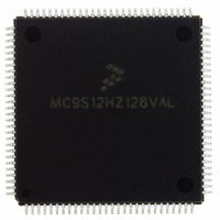
MC9S12HZ128VAL
Manufacturer Part Number
MC9S12HZ128VAL
Description
IC MCU 16BIT 2K FLASH 112-LQFP
Manufacturer
Freescale Semiconductor
Series
HCS12r
Datasheet
1.MC9S12HZ128CAL.pdf
(692 pages)
Specifications of MC9S12HZ128VAL
Core Processor
HCS12
Core Size
16-Bit
Speed
25MHz
Connectivity
CAN, EBI/EMI, I²C, SCI, SPI
Peripherals
LCD, Motor control PWM, POR, PWM, WDT
Number Of I /o
85
Program Memory Size
128KB (128K x 8)
Program Memory Type
FLASH
Eeprom Size
2K x 8
Ram Size
6K x 8
Voltage - Supply (vcc/vdd)
2.35 V ~ 5.5 V
Data Converters
A/D 16x10b
Oscillator Type
Internal
Operating Temperature
-40°C ~ 105°C
Package / Case
112-LQFP
Processor Series
S12H
Core
HCS12
Data Bus Width
16 bit
Data Ram Size
6 KB
Interface Type
I2C/SCI/SPI
Maximum Clock Frequency
50 MHz
Number Of Programmable I/os
85
Number Of Timers
8
Maximum Operating Temperature
+ 105 C
Mounting Style
SMD/SMT
3rd Party Development Tools
EWHCS12
Minimum Operating Temperature
- 40 C
On-chip Adc
16-ch x 10-bit
Lead Free Status / RoHS Status
Lead free / RoHS Compliant
Available stocks
Company
Part Number
Manufacturer
Quantity
Price
Company:

Part Number:
MC9S12HZ128VAL
Manufacturer:
Freescale Semiconductor
Quantity:
10 000
Part Number:
MC9S12HZ128VAL
Manufacturer:
FREESCALE
Quantity:
20 000


Chapter 19 Debug Module (DBGV1)
19.3.2.1
542
TRGSEL
DBGEN
Reset
BEGIN
Field
ARM
7
6
5
4
W
R
DBGEN
DBG Mode Enable Bit — The DBGEN bit enables the DBG module for use in DBG mode. This bit cannot be
set if the MCU is in secure mode.
0 DBG mode disabled
1 DBG mode enabled
Arm Bit — The ARM bit controls whether the debugger is comparing and storing data in the trace buffer. See
Section 19.4.2.4, “Arming the DBG
0 Debugger unarmed
1 Debugger armed
Note: This bit cannot be set if the DBGEN bit is not also being set at the same time. For example, a write of 01
Trigger Selection Bit — The TRGSEL bit controls the triggering condition for comparators A and B in DBG
mode. It serves essentially the same function as the TAGAB bit in the DBGC2 register does in BKP mode. See
Section 19.4.2.1.2, “Trigger
based on comparator A and B if enabled in DBG mode (DBGBRK = 1). Please refer to
“Breakpoint Based on Comparator A and
0 Trigger on any compare address match
1 Trigger before opcode at compare address gets executed (tagged-type)
Begin/End Trigger Bit — The BEGIN bit controls whether the trigger begins or ends storing of data in the trace
buffer. See
for more details.
0 Trigger at end of stored data
1 Trigger before storing data
Debug Control Register 1 (DBGC1)
0
7
All bits are used in DBG mode only.
This register cannot be written if BKP mode is enabled (BKABEN in
DBGC2 is set).
to DBGEN[7:6] will be interpreted as a write of 00.
= Unimplemented or Reserved
Section 19.4.2.8.1, “Storing with
ARM
0
6
Figure 19-4. Debug Control Register (DBGC1)
Table 19-3. DBGC1 Field Descriptions
TRGSEL
Selection,” for more information. TRGSEL may also determine the type of breakpoint
MC9S12HZ256 Data Sheet, Rev. 2.05
0
5
Module,” for more information.
B.”
BEGIN
NOTE
NOTE
Begin-Trigger,” and
0
4
Description
DBGBRK
0
3
Section 19.4.2.8.2, “Storing with
0
0
2
Freescale Semiconductor
Section 19.4.3.1,
0
1
CAPMOD
End-Trigger,”
0
0
Related parts for MC9S12HZ128VAL
Image
Part Number
Description
Manufacturer
Datasheet
Request
R

Part Number:
Description:
Manufacturer:
Freescale Semiconductor, Inc
Datasheet:
Part Number:
Description:
Manufacturer:
Freescale Semiconductor, Inc
Datasheet:
Part Number:
Description:
Manufacturer:
Freescale Semiconductor, Inc
Datasheet:
Part Number:
Description:
Manufacturer:
Freescale Semiconductor, Inc
Datasheet:
Part Number:
Description:
Manufacturer:
Freescale Semiconductor, Inc
Datasheet:
Part Number:
Description:
Manufacturer:
Freescale Semiconductor, Inc
Datasheet:
Part Number:
Description:
Manufacturer:
Freescale Semiconductor, Inc
Datasheet:
Part Number:
Description:
Manufacturer:
Freescale Semiconductor, Inc
Datasheet:
Part Number:
Description:
Manufacturer:
Freescale Semiconductor, Inc
Datasheet:
Part Number:
Description:
Manufacturer:
Freescale Semiconductor, Inc
Datasheet:
Part Number:
Description:
Manufacturer:
Freescale Semiconductor, Inc
Datasheet:
Part Number:
Description:
Manufacturer:
Freescale Semiconductor, Inc
Datasheet:
Part Number:
Description:
Manufacturer:
Freescale Semiconductor, Inc
Datasheet:
Part Number:
Description:
Manufacturer:
Freescale Semiconductor, Inc
Datasheet:
Part Number:
Description:
Manufacturer:
Freescale Semiconductor, Inc
Datasheet: