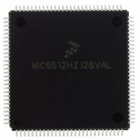
MC9S12HZ128VAL Freescale Semiconductor, MC9S12HZ128VAL Datasheet - Page 377

MC9S12HZ128VAL
Manufacturer Part Number
MC9S12HZ128VAL
Description
IC MCU 16BIT 2K FLASH 112-LQFP
Manufacturer
Freescale Semiconductor
Series
HCS12r
Datasheet
1.MC9S12HZ128CAL.pdf
(692 pages)
Specifications of MC9S12HZ128VAL
Core Processor
HCS12
Core Size
16-Bit
Speed
25MHz
Connectivity
CAN, EBI/EMI, I²C, SCI, SPI
Peripherals
LCD, Motor control PWM, POR, PWM, WDT
Number Of I /o
85
Program Memory Size
128KB (128K x 8)
Program Memory Type
FLASH
Eeprom Size
2K x 8
Ram Size
6K x 8
Voltage - Supply (vcc/vdd)
2.35 V ~ 5.5 V
Data Converters
A/D 16x10b
Oscillator Type
Internal
Operating Temperature
-40°C ~ 105°C
Package / Case
112-LQFP
Processor Series
S12H
Core
HCS12
Data Bus Width
16 bit
Data Ram Size
6 KB
Interface Type
I2C/SCI/SPI
Maximum Clock Frequency
50 MHz
Number Of Programmable I/os
85
Number Of Timers
8
Maximum Operating Temperature
+ 105 C
Mounting Style
SMD/SMT
3rd Party Development Tools
EWHCS12
Minimum Operating Temperature
- 40 C
On-chip Adc
16-ch x 10-bit
Lead Free Status / RoHS Status
Lead free / RoHS Compliant
Available stocks
Company
Part Number
Manufacturer
Quantity
Price
Company:
Part Number:
MC9S12HZ128VAL
Manufacturer:
Freescale Semiconductor
Quantity:
10 000
Part Number:
MC9S12HZ128VAL
Manufacturer:
FREESCALE
Quantity:
20 000
- Current page: 377 of 692
- Download datasheet (4Mb)
The synchronization jump width (see the Bosch CAN specification for details) can be programmed in a
range of 1 to 4 time quanta by setting the SJW parameter.
The SYNC_SEG, TSEG1, TSEG2, and SJW parameters are set by programming the MSCAN bus timing
registers (CANBTR0, CANBTR1) (see
and
Table 12-36
12.4.4
The MSCAN generates an internal time stamp whenever a valid frame is received or transmitted and the
TIME bit is enabled. Because the CAN specification defines a frame to be valid if no errors occur before
the end of frame (EOF) field is transmitted successfully, the actual value of an internal timer is written at
EOF to the appropriate time stamp position within the transmit buffer. For receive frames, the time stamp
is written to the receive buffer.
Freescale Semiconductor
Section 12.3.2.4, “MSCAN Bus Timing Register 1
Time Segment 1
Timer Link
gives an overview of the CAN compliant segment settings and the related parameter values.
5 .. 10
4 .. 11
5 .. 12
6 .. 13
7 .. 14
8 .. 15
9 .. 16
It is the user’s responsibility to ensure the bit time settings are in compliance
with the CAN standard.
Transmit Point
Sample Point
SYNC_SEG
Syntax
Table 12-36. CAN Standard Compliant Bit Time Segment Settings
TSEG1
3 .. 10
4 .. 11
5 .. 12
6 .. 13
7 .. 14
8 .. 15
4 .. 9
System expects transitions to occur on the CAN bus during this
period.
A node in transmit mode transfers a new value to the CAN bus at
this point.
A node in receive mode samples the CAN bus at this point. If the
three samples per bit option is selected, then this point marks the
position of the third sample.
Table 12-35. Time Segment Syntax
MC9S12HZ256 Data Sheet, Rev. 2.05
Time Segment 2
Section 12.3.2.3, “MSCAN Bus Timing Register 0
2
3
4
5
6
7
8
NOTE
Chapter 12 Freescale’s Scalable Controller Area Network (MSCANV2)
(CANBTR1)”).
Description
TSEG2
1
2
3
4
5
6
7
Synchronization
Jump Width
1 .. 2
1 .. 3
1 .. 4
1 .. 4
1 .. 4
1 .. 4
1 .. 4
(CANBTR0)”
SJW
0 .. 1
0 .. 2
0 .. 3
0 .. 3
0 .. 3
0 .. 3
0 .. 3
377
Related parts for MC9S12HZ128VAL
Image
Part Number
Description
Manufacturer
Datasheet
Request
R
Part Number:
Description:
Manufacturer:
Freescale Semiconductor, Inc
Datasheet:
Part Number:
Description:
Manufacturer:
Freescale Semiconductor, Inc
Datasheet:
Part Number:
Description:
Manufacturer:
Freescale Semiconductor, Inc
Datasheet:
Part Number:
Description:
Manufacturer:
Freescale Semiconductor, Inc
Datasheet:
Part Number:
Description:
Manufacturer:
Freescale Semiconductor, Inc
Datasheet:
Part Number:
Description:
Manufacturer:
Freescale Semiconductor, Inc
Datasheet:
Part Number:
Description:
Manufacturer:
Freescale Semiconductor, Inc
Datasheet:
Part Number:
Description:
Manufacturer:
Freescale Semiconductor, Inc
Datasheet:
Part Number:
Description:
Manufacturer:
Freescale Semiconductor, Inc
Datasheet:
Part Number:
Description:
Manufacturer:
Freescale Semiconductor, Inc
Datasheet:
Part Number:
Description:
Manufacturer:
Freescale Semiconductor, Inc
Datasheet:
Part Number:
Description:
Manufacturer:
Freescale Semiconductor, Inc
Datasheet:
Part Number:
Description:
Manufacturer:
Freescale Semiconductor, Inc
Datasheet:
Part Number:
Description:
Manufacturer:
Freescale Semiconductor, Inc
Datasheet:
Part Number:
Description:
Manufacturer:
Freescale Semiconductor, Inc
Datasheet:


