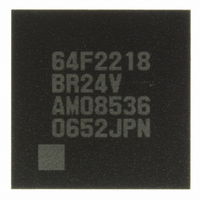
DF2218BR24V Renesas Electronics America, DF2218BR24V Datasheet - Page 123

DF2218BR24V
Manufacturer Part Number
DF2218BR24V
Description
IC H8S/2218 MCU FLASH 112-LFBGA
Manufacturer
Renesas Electronics America
Series
H8® H8S/2200r
Specifications of DF2218BR24V
Core Processor
H8S/2000
Core Size
16-Bit
Speed
24MHz
Connectivity
SCI, SmartCard, USB
Peripherals
DMA, POR, PWM, WDT
Number Of I /o
69
Program Memory Size
128KB (128K x 8)
Program Memory Type
FLASH
Ram Size
12K x 8
Voltage - Supply (vcc/vdd)
2.7 V ~ 3.6 V
Data Converters
A/D 6x10b
Oscillator Type
External
Operating Temperature
-20°C ~ 75°C
Package / Case
112-LFBGA
For Use With
HS0005KCU11H - EMULATOR E10A-USB H8S(X),SH2(A)3DK2218-SS - KIT DEV H8S/2218 WINDOWS SIDESHW3DK2218 - DEV EVAL KIT H8S/2218
Lead Free Status / RoHS Status
Lead free / RoHS Compliant
Eeprom Size
-
Available stocks
Company
Part Number
Manufacturer
Quantity
Price
Company:
Part Number:
DF2218BR24V
Manufacturer:
Renesas Electronics America
Quantity:
10 000
- Current page: 123 of 758
- Download datasheet (5Mb)
The instructions BSET, BCLR, BNOT, BST, and BIST perform the following operations in the
order shown:
1. Read data in byte units
2. Perform bit manipulation on the read data according to the instruction
3. Write data in byte units
Example: Using the BCLR instruction to clear pin 14 only of P1DDR for port 1
P1DDR is an 8-bit register that contains write-only bits. It is used to specify the I/O setting of the
individual pins in port 1. Reading produces invalid data. Attempting to read from P1DDR returns
undefined values.
In this example, the BCLR instruction is used to set pin 14 as an input port. Let us assume that pins
17 to 14 are presently set as output pins and pins 13 to 10 are set as input pins. Thus, the value of
P1DDR is initially H'F0.
I/O
P1DDR
To change pin 14 from an output pin to an input pin, the value of bit 4 in P1DDR must be changed
from 1 to 0 (H'F0 to H'E0). Now assume that the BCLR instruction is used to clear bit 4 in P1DDR
to 0.
However, using the above bit manipulation instruction on the write-only register P1DDR can cause
problems, as described below.
The BCLR instruction first reads data from P1DDR in byte units, but in this case the read values
are undefined. These undefined values can be 0 or 1 for each bit in the register, but there is no way
of telling which. Since all of the bits in P1DDR are write-only, undefined values are returned for
all of the bits when the register is read. In this example the value of P1DDR is H'F0, but we will
assume that the value returned when the register was read is H'F8, which would give bit 3 a value
of 1.
BCLR
#4, @P1DDR
P17
Output
1
P16
Output
1
P15
Output
1
P14
Output
1
P13
Input
0
Rev.7.00 Dec. 24, 2008 Page 67 of 698
P12
Input
0
P11
Input
0
REJ09B0074-0700
P10
Input
0
Related parts for DF2218BR24V
Image
Part Number
Description
Manufacturer
Datasheet
Request
R

Part Number:
Description:
CONN SOCKET 2POS 7.92MM WHITE
Manufacturer:
Hirose Electric Co Ltd
Datasheet:

Part Number:
Description:
CONN SOCKET 4POS 7.92MM WHITE
Manufacturer:
Hirose Electric Co Ltd
Datasheet:

Part Number:
Description:
CONN SOCKET 5POS 7.92MM WHITE
Manufacturer:
Hirose Electric Co Ltd
Datasheet:

Part Number:
Description:
CONN SOCKET 3POS 7.92MM WHITE
Manufacturer:
Hirose Electric Co Ltd
Datasheet:

Part Number:
Description:
CONN SOCKET 5POS 7.92MM WHITE
Manufacturer:
Hirose Electric Co Ltd
Datasheet:

Part Number:
Description:
CONN SOCKET 2POS 7.92MM WHITE
Manufacturer:
Hirose Electric Co Ltd
Datasheet:

Part Number:
Description:
CONN SOCKET 3POS 7.92MM WHITE
Manufacturer:
Hirose Electric Co Ltd
Datasheet:

Part Number:
Description:
CONN SOCKET 4POS 7.92MM WHITE
Manufacturer:
Hirose Electric Co Ltd
Datasheet:

Part Number:
Description:
CONN HEADER 2POS 7.92MM R/A TIN
Manufacturer:
Hirose Electric Co Ltd
Datasheet:

Part Number:
Description:
CONN HEADER 4POS 7.92MM R/A TIN
Manufacturer:
Hirose Electric Co Ltd
Datasheet:

Part Number:
Description:
KIT STARTER FOR M16C/29
Manufacturer:
Renesas Electronics America
Datasheet:

Part Number:
Description:
KIT STARTER FOR R8C/2D
Manufacturer:
Renesas Electronics America
Datasheet:

Part Number:
Description:
R0K33062P STARTER KIT
Manufacturer:
Renesas Electronics America
Datasheet:

Part Number:
Description:
KIT STARTER FOR R8C/23 E8A
Manufacturer:
Renesas Electronics America
Datasheet:

Part Number:
Description:
KIT STARTER FOR R8C/25
Manufacturer:
Renesas Electronics America
Datasheet:


