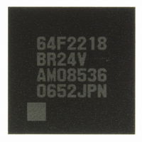
DF2218BR24V Renesas Electronics America, DF2218BR24V Datasheet - Page 661

DF2218BR24V
Manufacturer Part Number
DF2218BR24V
Description
IC H8S/2218 MCU FLASH 112-LFBGA
Manufacturer
Renesas Electronics America
Series
H8® H8S/2200r
Specifications of DF2218BR24V
Core Processor
H8S/2000
Core Size
16-Bit
Speed
24MHz
Connectivity
SCI, SmartCard, USB
Peripherals
DMA, POR, PWM, WDT
Number Of I /o
69
Program Memory Size
128KB (128K x 8)
Program Memory Type
FLASH
Ram Size
12K x 8
Voltage - Supply (vcc/vdd)
2.7 V ~ 3.6 V
Data Converters
A/D 6x10b
Oscillator Type
External
Operating Temperature
-20°C ~ 75°C
Package / Case
112-LFBGA
For Use With
HS0005KCU11H - EMULATOR E10A-USB H8S(X),SH2(A)3DK2218-SS - KIT DEV H8S/2218 WINDOWS SIDESHW3DK2218 - DEV EVAL KIT H8S/2218
Lead Free Status / RoHS Status
Lead free / RoHS Compliant
Eeprom Size
-
Available stocks
Company
Part Number
Manufacturer
Quantity
Price
Company:
Part Number:
DF2218BR24V
Manufacturer:
Renesas Electronics America
Quantity:
10 000
- Current page: 661 of 758
- Download datasheet (5Mb)
19.9
19.9.1
Since various characteristics related to the crystal resonator are closely linked to the user's board
design, thorough evaluation is necessary on the user's part, using the resonator connection
examples shown in this section as a guide. As the resonator circuit ratings will depend on the
floating capacitance of the resonator and the mounting circuit, the ratings should be determined in
consultation with the resonator manufacturer. The design must ensure that a voltage exceeding the
maximum rating is not applied to the oscillator pin.
19.9.2
When designing the board, place the crystal resonator and its load capacitors as close as possible to
the XTAL or OSC1 and EXTAL or OSC2 pins. Other signal lines should be routed away from the
oscillator circuit to prevent induction from interfering with correct oscillation. See figure 19.10.
19.9.3
When two or more external clocks (e.g. 16 MHz and 13 MHz) are used as the system clock,
switchover of the input clock should be carried out in software standby mode.
An example of an external clock switching circuit is shown in figure 19.11, and an example of the
external clock switchover timing in figure 19.12.
Usage Notes
Note on Crystal Resonator
Note on Board Design
Note on Switchover of External Clock
Figure 19.10 Note on Board Design of Oscillator Circuit
Prohibit
C
C
1
2
Signal A Signal B
Rev.7.00 Dec. 24, 2008 Page 605 of 698
EXTAL or
OSC1
XTAL or
OSC2
This LSI
REJ09B0074-0700
Related parts for DF2218BR24V
Image
Part Number
Description
Manufacturer
Datasheet
Request
R

Part Number:
Description:
CONN SOCKET 2POS 7.92MM WHITE
Manufacturer:
Hirose Electric Co Ltd
Datasheet:

Part Number:
Description:
CONN SOCKET 4POS 7.92MM WHITE
Manufacturer:
Hirose Electric Co Ltd
Datasheet:

Part Number:
Description:
CONN SOCKET 5POS 7.92MM WHITE
Manufacturer:
Hirose Electric Co Ltd
Datasheet:

Part Number:
Description:
CONN SOCKET 3POS 7.92MM WHITE
Manufacturer:
Hirose Electric Co Ltd
Datasheet:

Part Number:
Description:
CONN SOCKET 5POS 7.92MM WHITE
Manufacturer:
Hirose Electric Co Ltd
Datasheet:

Part Number:
Description:
CONN SOCKET 2POS 7.92MM WHITE
Manufacturer:
Hirose Electric Co Ltd
Datasheet:

Part Number:
Description:
CONN SOCKET 3POS 7.92MM WHITE
Manufacturer:
Hirose Electric Co Ltd
Datasheet:

Part Number:
Description:
CONN SOCKET 4POS 7.92MM WHITE
Manufacturer:
Hirose Electric Co Ltd
Datasheet:

Part Number:
Description:
CONN HEADER 2POS 7.92MM R/A TIN
Manufacturer:
Hirose Electric Co Ltd
Datasheet:

Part Number:
Description:
CONN HEADER 4POS 7.92MM R/A TIN
Manufacturer:
Hirose Electric Co Ltd
Datasheet:

Part Number:
Description:
KIT STARTER FOR M16C/29
Manufacturer:
Renesas Electronics America
Datasheet:

Part Number:
Description:
KIT STARTER FOR R8C/2D
Manufacturer:
Renesas Electronics America
Datasheet:

Part Number:
Description:
R0K33062P STARTER KIT
Manufacturer:
Renesas Electronics America
Datasheet:

Part Number:
Description:
KIT STARTER FOR R8C/23 E8A
Manufacturer:
Renesas Electronics America
Datasheet:

Part Number:
Description:
KIT STARTER FOR R8C/25
Manufacturer:
Renesas Electronics America
Datasheet:


